Process for manufacturing a semiconductor chip

a manufacturing process and semiconductor technology, applied in the direction of manufacturing tools, laminated machines, solid-state devices, etc., can solve the problems of not being able to carry out the bonding work smoothly, the adhesive film cannot be affixed to the back surface of the semiconductor wafer beforehand, and the adhesive film cannot be cu

Active Publication Date: 2005-09-06
DISCO CORP
View PDF5 Cites 28 Cited by
  • Summary
  • Abstract
  • Description
  • Claims
  • Application Information

AI Technical Summary

Benefits of technology

[0008]It is an object of the present invention to provide a semiconductor chip manufacturing process which enables an adhesive film for die bonding to be affixed to the back surface of semiconductor chips easily without damaging the front surface of the individual semiconductor chips obtained by dividing a semiconductor wafer by pre-dicing.

Problems solved by technology

The adhesive film for die bonding, therefore, cannot be affixed onto the back surface of the semiconductor wafer beforehand.
This poses a problem making it impossible to carry out the bonding work smoothly.
However, it is difficult to cut only the adhesive film without applying a laser beam to the front surfaces of the semiconductor chips.
Therefore, in the semiconductor chip manufacturing process disclosed by the above publication, the front surfaces of the semiconductor chips having a circuit formed thereon might have damage by the laser beam.

Method used


Image

  • Process for manufacturing a semiconductor chip
  • Process for manufacturing a semiconductor chip
  • Process for manufacturing a semiconductor chip

Examples


Embodiment Construction

[0034]A preferred embodiment of the semiconductor chip manufacturing process according to the present invention will be described in detail hereinbelow with reference to the accompanying drawings.

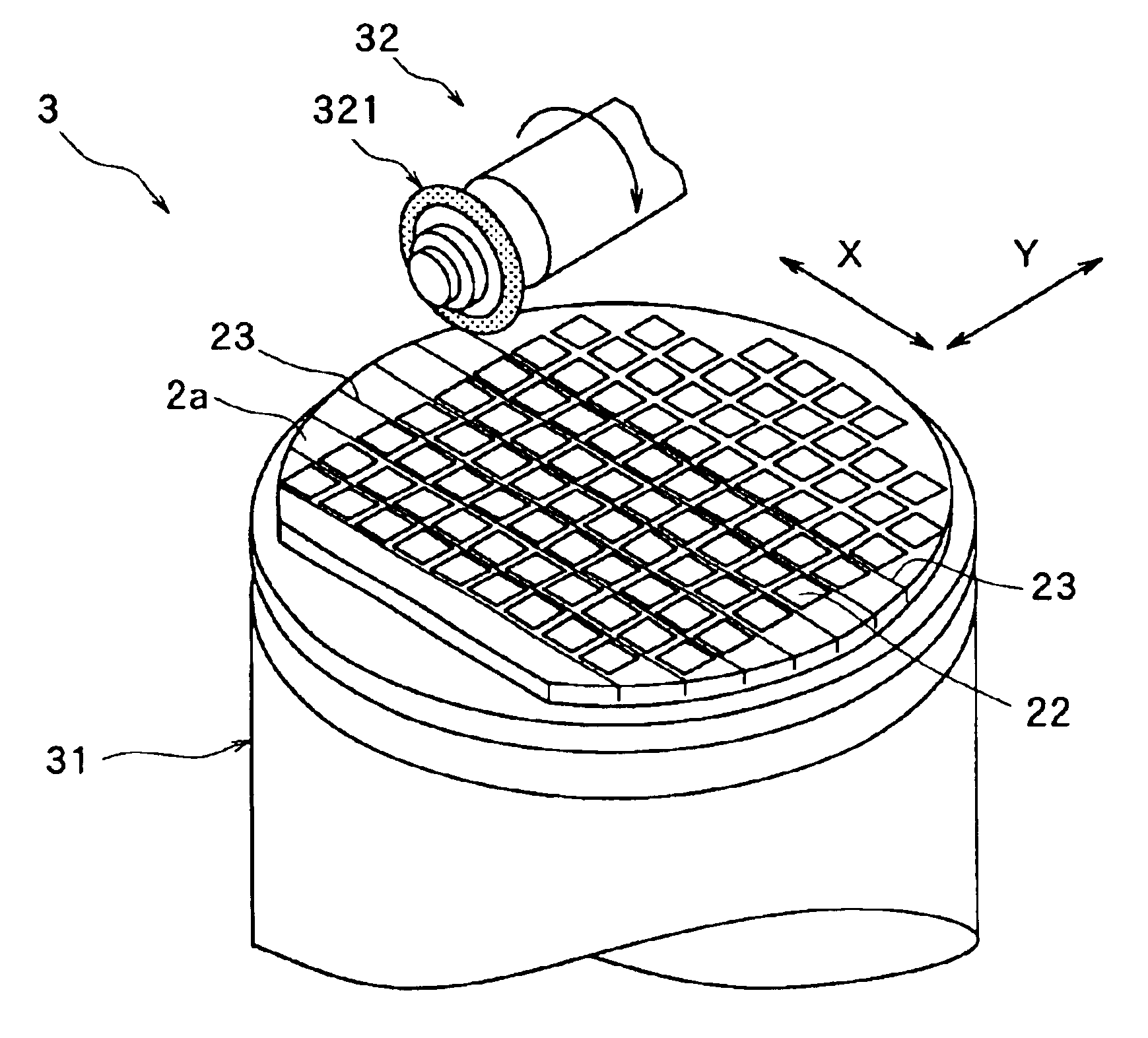
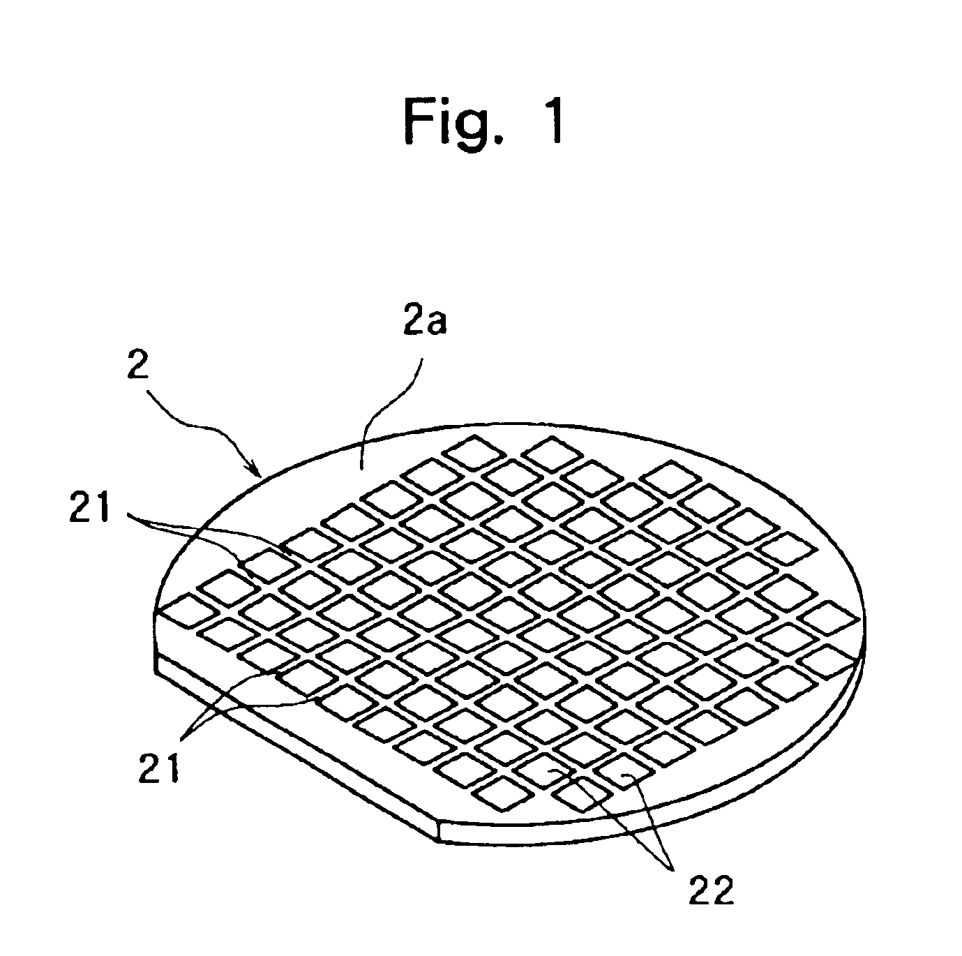
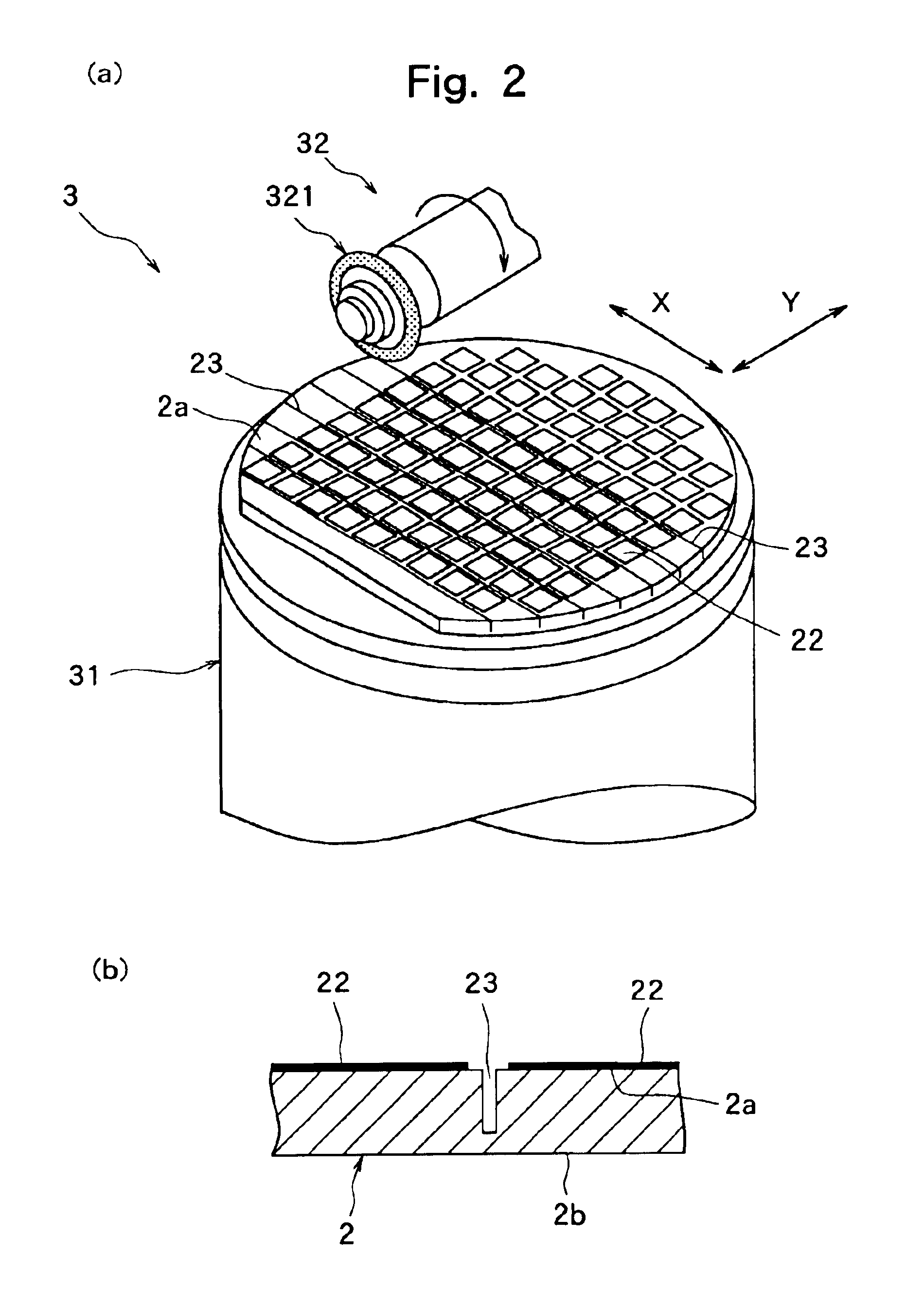
[0035]FIG. 1 is a perspective view of a semiconductor wafer to be divided according to the present invention. The semiconductor wafer 2 shown in FIG. 1 has a plurality of streets 21 formed in a lattice-like form on the front surface 2a and circuits 22 formed in a plurality of areas sectioned by the plurality of streets 21. The process for manufacturing semiconductor chips by dividing this semiconductor wafer 2 into individual semiconductor chips will be described with reference to FIGS. 2 to 10.

[0036]To divide the semiconductor wafer 2 into individual semiconductor chips, dividing grooves having a predetermined depth (corresponding to the final thickness of each semiconductor chip) are first formed along the streets 21 formed on the front surface 2a of the semiconductor wafer 2 (dividing gr...


PUM

PropertyMeasurementUnit
thicknessaaaaaaaaaa
thicknessaaaaaaaaaa
thicknessaaaaaaaaaa

Abstract

A process for manufacturing a semiconductor chip by dividing a semiconductor wafer having a plurality of streets formed in a lattice-like form on the front surface into individual semiconductor chips, and affixing an adhesive film for die bonding to the back surfaces of the individual semiconductor chips, comprising a dividing groove forming step for forming dividing grooves having a predetermined depth from the front surface of the semiconductor wafer along the streets; a protective member affixing step for affixing a protective member to the front surface having dividing grooves formed thereon of the semiconductor wafer; a dividing groove exposing step for exposing the dividing grooves to the back surface by grinding the back surface of the semiconductor wafer to divide the semiconductor wafer into individual semiconductor chips; an adhesive film affixing step for affixing the adhesive film to the back surfaces of the individually divided semiconductor chips; and an adhesive film cutting step for applying a laser beam to the adhesive film affixed on the back surfaces of the individually divided semiconductor chips from the front surface side of the adhesive film along the dividing grooves to cut the adhesive film along the dividing grooves.

Description

FIELD OF THE INVENTION[0001]The present invention relates to a process for manufacturing a semiconductor chip by dividing a semiconductor wafer having a plurality of streets formed in a lattice-like form on the front surface and circuits formed in a plurality of areas sectioned by the plurality of streets, into individual semiconductor chips and affixing an adhesive film for die bonding to the back surfaces of the individual semiconductor chips.DESCRIPTION OF THE PRIOR ART[0002]In the production process of a semiconductor device, for example, individual semiconductor chips are manufactured by forming a circuit such as IC or LSI in a plurality of areas sectioned by streets (cutting lines) formed in a lattice-like form on the front surface of a substantially disk-like semiconductor wafer, and dividing the semiconductor wafer into the circuit formed areas along the streets. A dicing machine is generally used as a dividing machine for dividing the semiconductor wafer to cut the semicond...

Claims


Application Information

Patent Timeline
Patent Type & Authority Patents(United States)
IPC IPC(8): B24B1/00B23K26/00B28D5/00B24B37/04H01L21/70H01L21/02H01L21/52H01L21/30H01L21/301H01L21/304H01L21/44H01L21/78H01L21/58H01L21/68
CPCH01L21/6835H01L21/6836H01L21/78H01L24/83H01L24/27H01L24/29H01L2221/68327H01L2221/68336H01L2224/274H01L2224/83191H01L2224/8385H01L2924/01004H01L2924/01005H01L2924/01033H01L2924/01039H01L2924/07802H01L2924/14H01L2924/01006H01L2924/01068Y10S438/928H01L2924/3512H01L2924/00H01L2924/12042
Inventor KAJIYAMA, KEIICHIODANAKA, KENTARO
Owner DISCO CORP
Why Eureka
Try Eureka