Apparatus for manufacturing semiconductor devices with a moveable shield

a technology of moving shields and semiconductor devices, applied in electrical apparatus, decorative surface effects, decorative arts, etc., can solve the problems of large amount of etchant consumed and long work time, and achieve the effect of quick and easy etching only a wafer edge and easy etching of a wafer edge edg

a technology of moving shields and semiconductor devices, applied in electrical apparatus, decorative surface effects, decorative arts, etc., can solve the problems of large amount of etchant consumed and long work time, and achieve the effect of quick and easy etching only a wafer edge and easy etching of a wafer edge edg

US6939807B2Inactive Publication Date: 2005-09-06SEMES CO LTD

Image

  • Apparatus for manufacturing semiconductor devices with a moveable shield
  • Apparatus for manufacturing semiconductor devices with a moveable shield
  • Apparatus for manufacturing semiconductor devices with a moveable shield

Examples


Embodiment Construction

[0026]The present invention will now be describe more fully hereinafter with reference to the accompanying drawings, in which preferred embodiments of the invention are shown. Like numbers refer to like elements throughout.

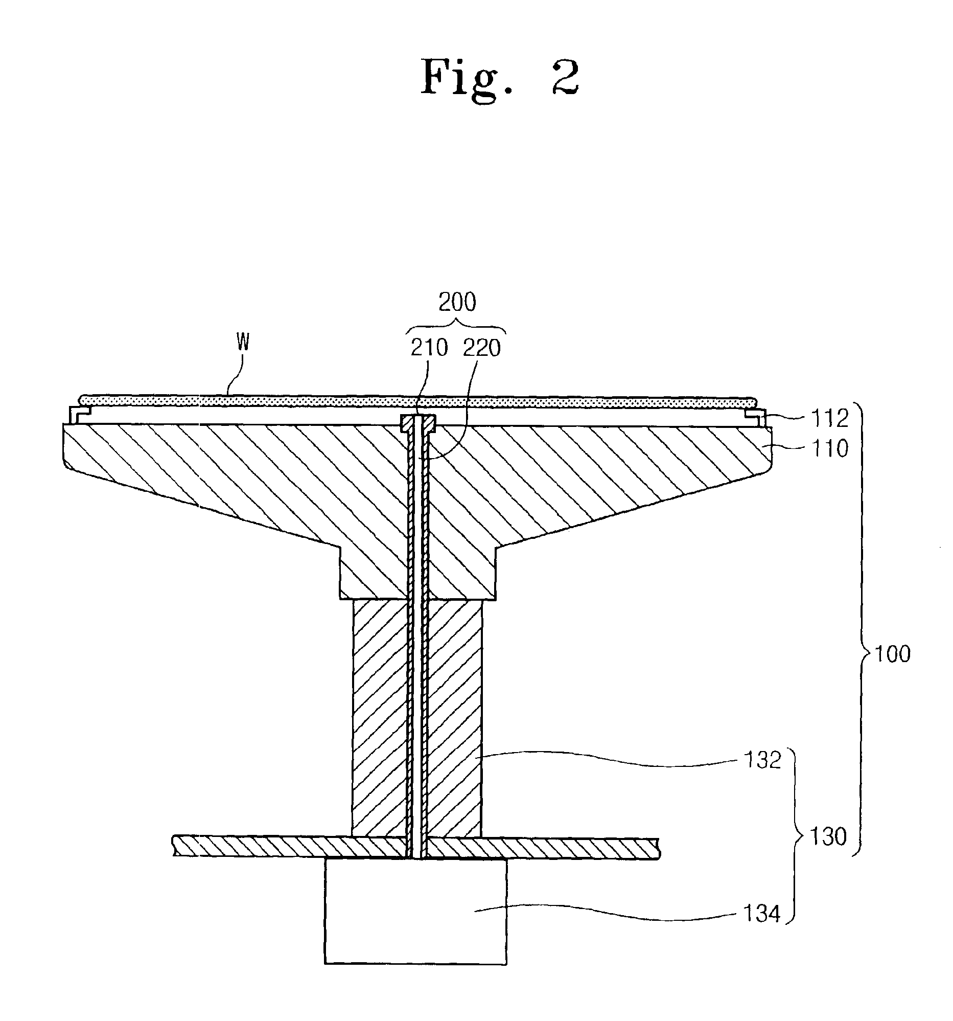
[0027]In the present invention, a top surface of a wafer means a surface on which a pattern is formed, and a bottom surface thereof means an opposite surface to the top surface. Further, a shielding portion means a wafer top surface except a wafer edge where incomplete chips are disposed and is shielded from a chemical solution injected to the edge.

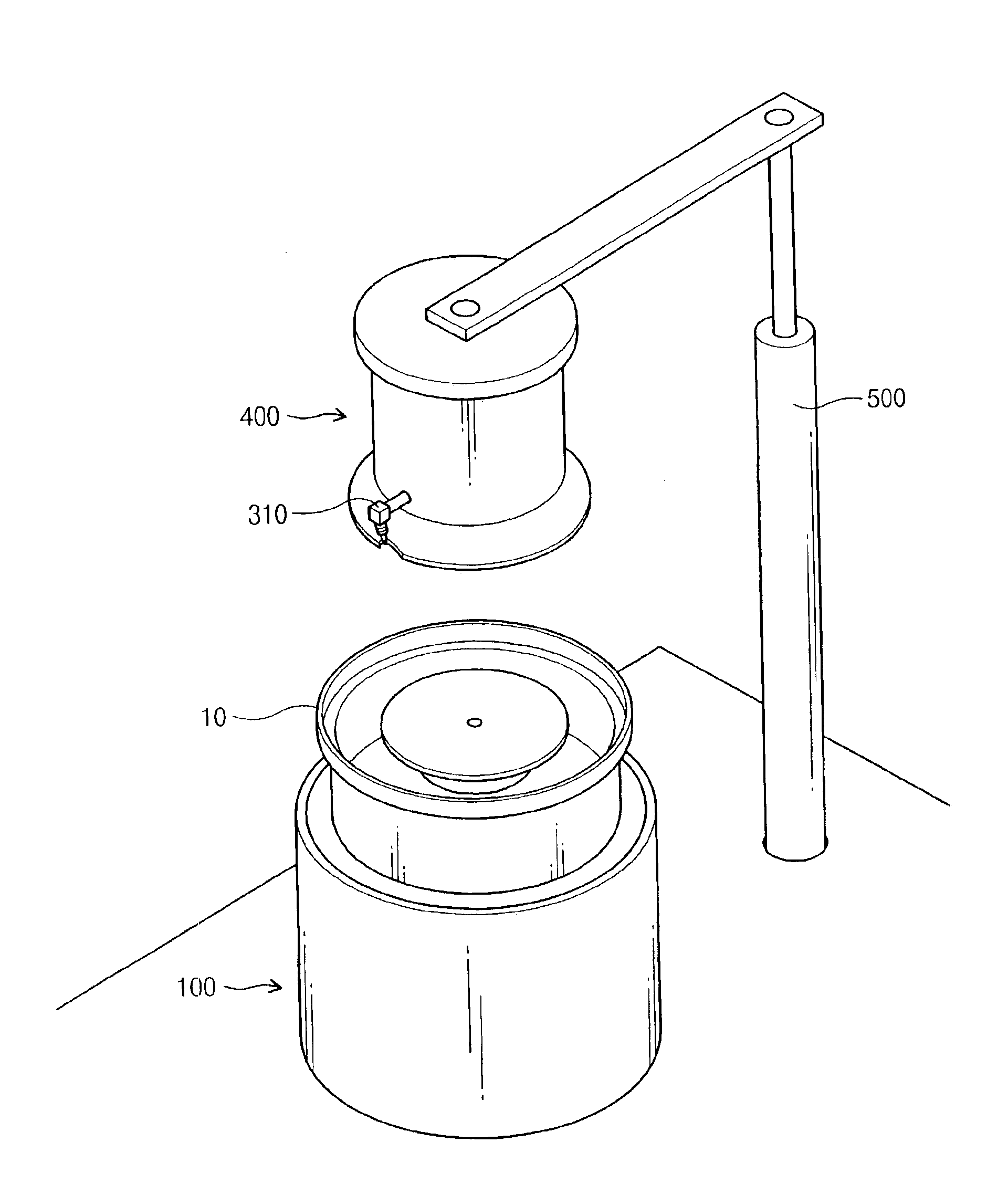
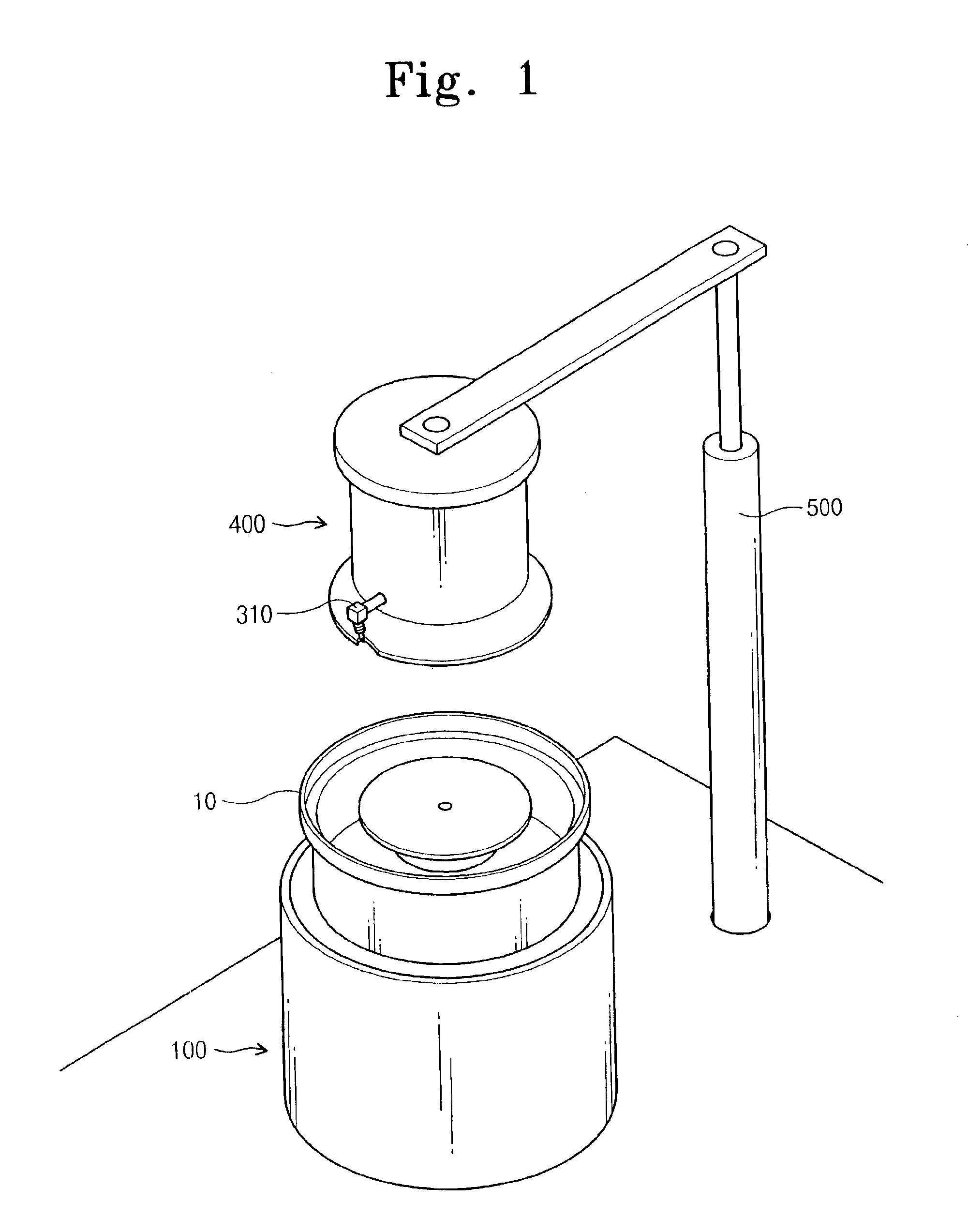
[0028]Although an etching apparatus will be exemplarily described in these embodiments, it may be applied to all semiconductor manufacturing apparatuses injecting a chemical solution only onto a wafer edge or a wafer lower portion.

[0029]A perspective view of an etching apparatus according to an embodiment of the present invention is illustrated in FIG. 1, and a supporter portion and a fluid injecting portion of FIG. 1 a...


PUM

PropertyMeasurementUnit
Distanceaaaaaaaaaa

Abstract

An apparatus for manufacturing semiconductor devices includes a supporter portion on which a semiconductor substrate is placed, a nozzle portion for injecting a fluid to an edge of the substrate placed on the supporter portion, a shielding cover for preventing the fluid injected from the nozzle portion from flowing to a shielding portion among a pattern-formed portion, and a shielding cover moving portion device for moving the shielding cover up and down. The apparatus makes it possible to prevent a chemical solution injected to the edge of a wafer from flowing to a shielding portion of the wafer when the wafer edge is etched.

Description

FIELD OF THE INVENTION[0001]The present invention relates to an apparatus for manufacturing semiconductor devices and, more particularly, to an etching apparatus for etching a pattern-formed portion except a predetermined region of a semiconductor substrate.BACKGROUND OF THE INVENTION[0002]In fabrication of semiconductor devices, a plurality of layers (e.g., a polysilicon layer, an oxide layer, a nitride layer, a metal layer, etc.) are formed on a wafer used as a semiconductor substrate. A photoresist layer is coated on the layer. By an exposure process, a pattern formed on a photomask is transcribed onto the photoresist layer. By an etching process, a desirable pattern is then formed on the wafer.[0003]Layers or photoresist remains at the edge of the wafer where these processes are carried out. In this case, if the wafer is held and transported to a different process, the remaining layers are spattered. Since they act as particles to reduce a yield, there is a need for an etching p...

Claims


Application Information

Patent Timeline
06 Sep 2005
Publication
US6939807B2
IPC
H01L21/00; H01L21/306
CPC
H01L21/6708; H01L21/306
Inventors
YUN, GWANG-UI; HAN, JAE-SUN