

Semiconductor device and semiconductor memory device provided with internal current setting adjustment circuit
a technology of current setting and semiconductor memory, which is applied in the direction of semiconductor devices, digital storage, instruments, etc., to achieve the effect of preventing an increase in power consumption and simple circuit configuration
- Summary
- Abstract
- Description
- Claims
- Application Information
AI Technical Summary
Benefits of technology
Problems solved by technology
Method used
Image

Examples
first embodiment
[0067
[0068](Overall Configuration)
[0069]The semiconductor device according to the first embodiment of the present invention is generally described with reference to FIGS. 1-3. In the description below, a signal prefixed by “ / ” represents an inverse signal of the corresponding signal without the prefix “ / ”.
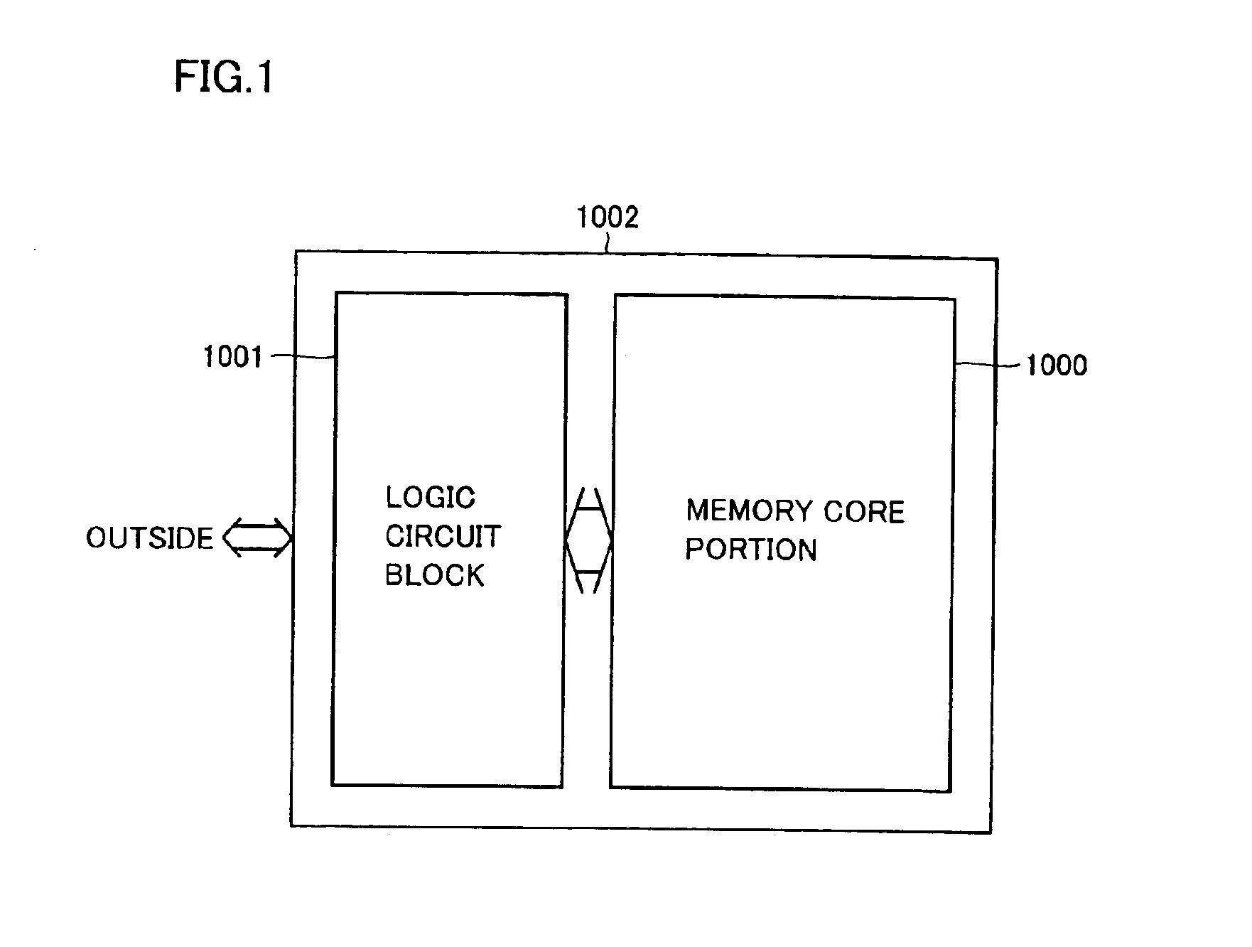
[0070]As shown in FIG. 1, the semiconductor device according to the first embodiment is provided with a memory core portion 1000 and a logic circuit block 1001. Memory core portion 1000 and logic circuit block 1001 are formed on a same chip 1002. Although not shown, SRAM, gate array, FPGA, nonvolatile RAM, ROM and others may also be mounted thereon.
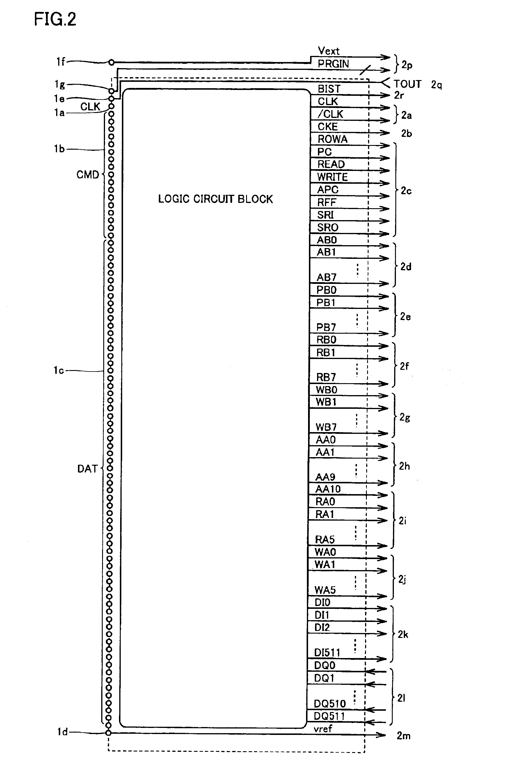
[0071]As shown in FIG. 2, logic circuit block 1001 and memory core portion 1000 perform signal transmission / reception via connect nodes 2a-2m, 2p-2r. Commands, addresses and data are transmitted from logic circuit block 1001 to memory core portion 1000, and correspondingly, data are transmitted from memory core portion 1000 to logic circ...
second embodiment
[0162
[0163]In the second embodiment, the configuration of a leakage current control circuit is described which is formed of a combination of the internal voltage control circuit and the leakage detecting circuit shown in the first embodiment and which has both functions to evaluate and adjust the leakage current.
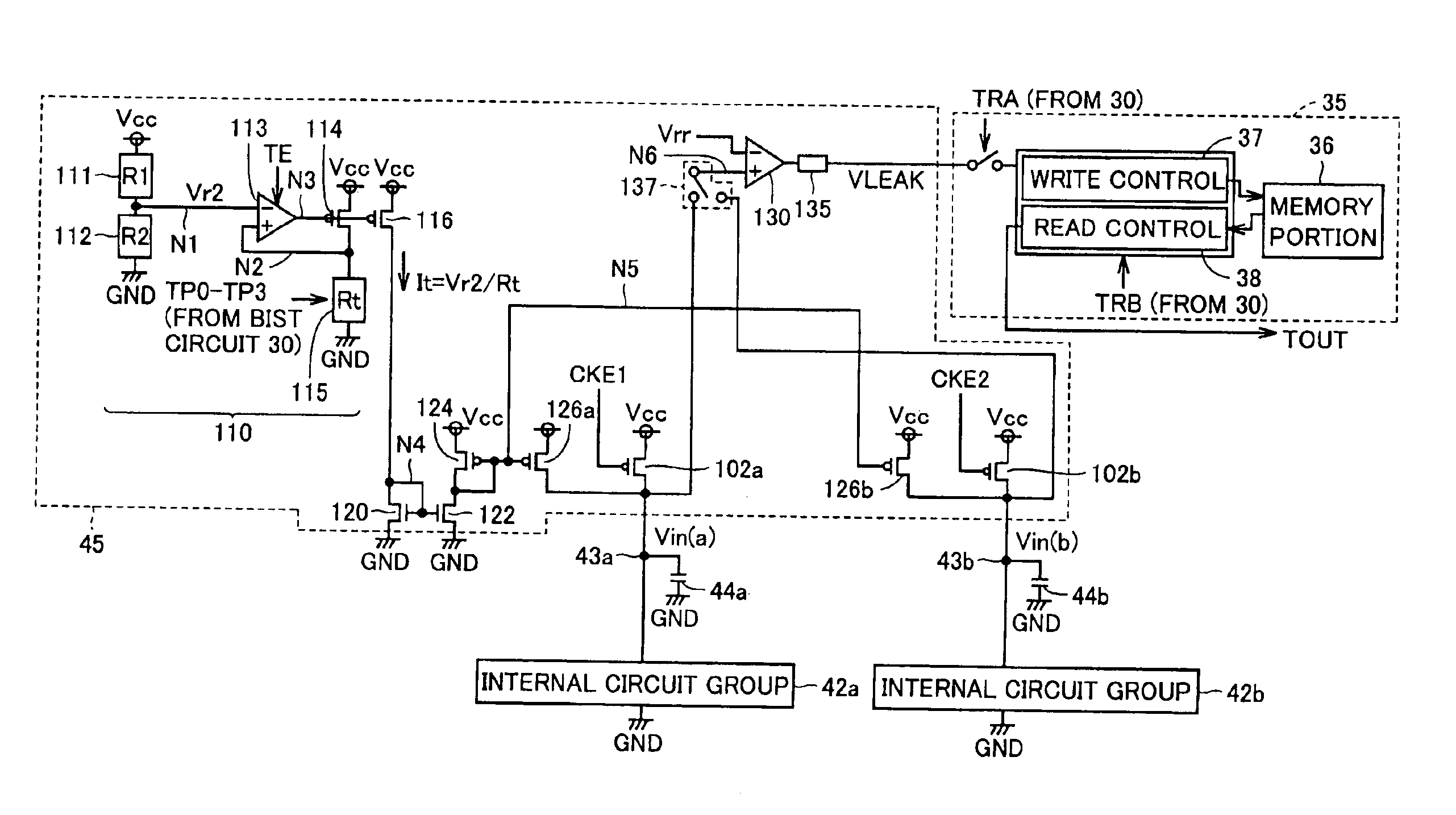
[0164]Referring to FIG. 10, the leakage current control circuit 100 according to the second embodiment includes internal voltage control circuit 40 shown in FIG. 4 and leakage detecting circuit 45 shown in FIG. 9.
[0165]Leakage detecting circuit 45 provides internal circuit group 42 with test current It adjustable in accordance with adjustment signals TP0-TP3 from BIST circuit 30, to determine whether the leakage current in internal circuit group 42 is greater than a specification value.
[0166]Internal voltage control circuit 40 responds to adjustment signals P0-P3 supplied from BIST circuit 30 or program circuit 31, and controls internal voltage Vbb which corresponds to the s...
third embodiment
[0191
[0192]In the third embodiment, a configuration for adjusting a data write current level in an MRAM device employing the internal voltage control circuit explained in the first embodiment, is described.
[0193]FIG. 14 is a first diagram showing a configuration associated with data write of the MRAM device according to the third embodiment.
[0194]Referring to FIG. 14, the MRAM device according to the third embodiment is provided with a memory cell array 210, row decoders 215W, 215R, a write digit line drive circuit 220, a word line driver 230, and a Vpp generating circuit 40#.
[0195]Memory cell array 210 has a plurality of MTJ memory cells MC arranged in rows and columns. Here, the configuration and data principle of the MTJ memory cell are described.
[0196]FIG. 15 is a conceptual diagram illustrating the structure and the data storage principle of the MTJ memory cell.
[0197]Referring to FIG. 15, a tunneling magneto-resistance element TMR has a ferromagnetic material layer having a fix...
PUM
 Abstract
Description
Claims
Application Information