Chip protection register unlocking

a technology of protection register and chip, applied in the field of integrated circuits, can solve the problems of not being reprogrammable, not properly removing the charge from the floating gate, and losing whatever data in the ram

Active Publication Date: 2005-09-20
MICRON TECH INC
View PDF10 Cites 17 Cited by
  • Summary
  • Abstract
  • Description
  • Claims
  • Application Information

AI Technical Summary

Benefits of technology

[0023]In a further embodiment, a method of operating a Flash memory device enables erasure of one or more lock bits associated with a protection register when the ...

Problems solved by technology

Most RAM is volatile, which means that it requires a steady flow of electricity to maintain its contents.
As soon as the power is turned off, whatever data was in RAM is lost.
Write fatigue is where the floating gate memory cell, after repetitive writes and erasures, no longer properly erases and removes charge from the floating gate.
A problem with protection registers and their associated lock bit(s) in Flash memories is that they are not re-programmable.
This can cause issues during manufacture of the Flash memory itself as the protection register and the associated lock bit(s) may be inadvertently programmed with an erroneous device ID or code due to mistake or an organizational or marketing change.
The Flash memory devices resulting from such inadvertent protec...

Method used


Image

  • Chip protection register unlocking
  • Chip protection register unlocking
  • Chip protection register unlocking

Examples


Embodiment Construction

[0031]In the following detailed description of the preferred embodiments, reference is made to the accompanying drawings that form a part hereof, and in which is shown by way of illustration specific preferred embodiments in which the inventions may be practiced. These embodiments are described in sufficient detail to enable those skilled in the art to practice the invention, and it is to be understood that other embodiments may be utilized and that logical, mechanical and electrical changes may be made without departing from the spirit and scope of the present invention. The following detailed description is, therefore, not to be taken in a limiting sense, and the scope of the present invention is defined only by the claims.

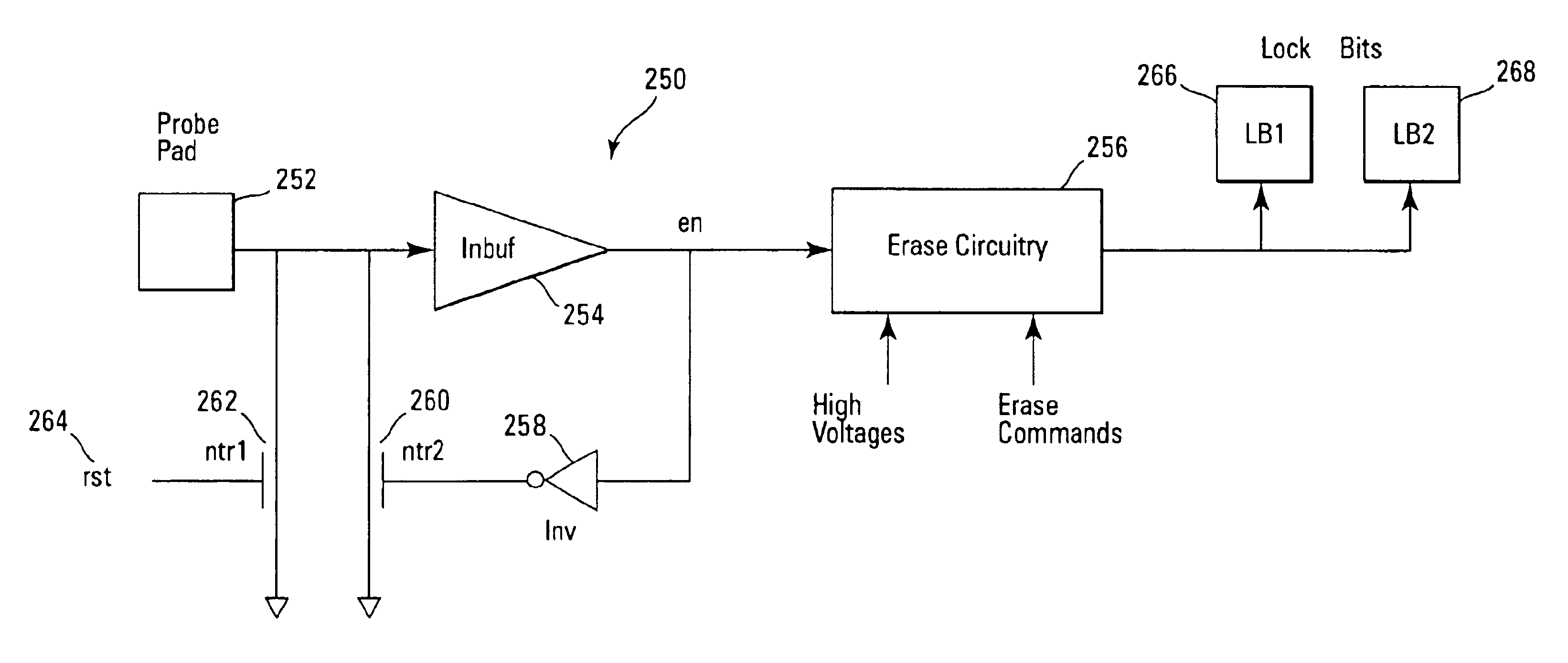
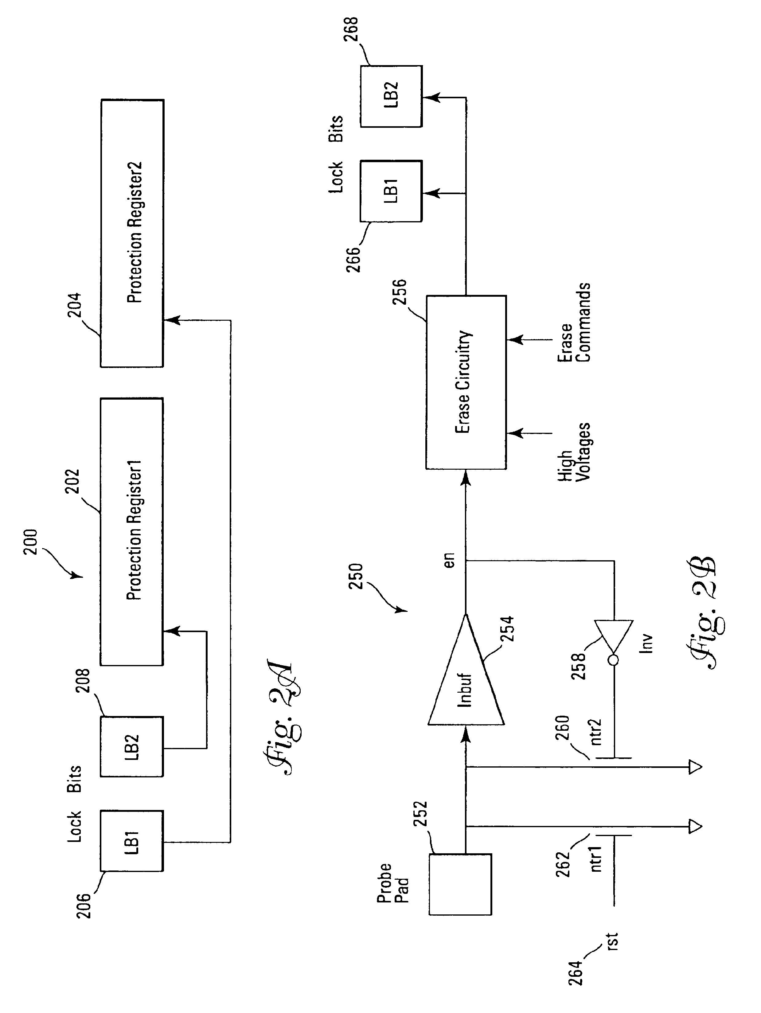
[0032]To improve manufacturing flexibility and allow for reprogramming of an erroneous device ID or code due to mistake, organizational, or marketing change a Flash memory of the present invention has a protection register and associated lock bit(s) that can be ...


PUM


Abstract

An improved Flash memory device is described with a protection register lock bit erase enable circuit. A bond pad coupled to the lock bit erase enable circuit of the improved Flash memory is not bonded when the individual Flash memory chip wafer is packaged. This allows the memory manufacturer to access the bond pad and erase the lock bits while the chip is still in wafer form via a test card probe, but makes the lock bits effectively uneraseable when the chip wafer is packaged. This enables the memory chip manufacturer to enhance reliability and fault tolerance of the Flash memory device by thoroughly testing the lock bits and protection register functionality. Additionally, the lock bit erase enable circuit increases manufacturing flexibility by allowing the memory chip manufacturer to reprogram the protection register and lock bits in case of organizational changes or inadvertent or erroneous programming of the protection register.

Description

RELATED APPLICATION[0001]This application claims priority to Italian Patent Application Serial No. RM2003A000039, filed Jan. 30, 2003, entitled “CHIP PROTECTION REGISTER UNLOCKING,” which is commonly assigned.[0002]1. Technical Field of the Invention[0003]The present invention relates generally to integrated circuits and in particular the present invention relates to protection registers of Flash memory devices.[0004]2. Background of the Invention[0005]Memory devices are typically provided as internal storage areas in the computer. The term memory identifies data storage that comes in the form of integrated circuit chips. There are several different types of memory used in modern electronics, one common type is RAM (random-access memory). RAM is characteristically found in use as main memory in a computer environment. RAM refers to read and write memory; that is, you can both write data into RAM and read data from RAM. This is in contrast to ROM, which permits you only to read data....

Claims


Application Information

Patent Timeline
IPC IPC(8): G11C16/00G11C16/04G11C17/00G11C7/24G11C16/22
CPCG11C7/24G11C16/22G11C2029/4402
Inventor NASO, GIOVANNIPIERSIMONI, PIETROVALI, TOMMASO
Owner MICRON TECH INC
Why Eureka
Try Eureka