Six-axis force sensor chip and six-axis force sensor using the same

a sensor chip and six-axis technology, applied in the direction of force/torque/work measurement apparatus, instruments, force measurement, etc., can solve the problems of low sensitivity of the sensor chip, the substrate of the semiconductor forming the sensor chip is susceptible to elastic deformation, etc., to reduce mutual interference, improve accuracy, robustness and reproducibility

Inactive Publication Date: 2005-10-04
HONDA MOTOR CO LTD
View PDF10 Cites 36 Cited by
  • Summary
  • Abstract
  • Description
  • Claims
  • Application Information

AI Technical Summary

Benefits of technology

[0047]It is, therefore, an object of the invention to solve the problems mentioned above and provide a six-axis force sensor chip and a six-axis force sensor using the same, which are capable of suppressing mutual interference among six-axis components of force or moment during detection and hence able to detect the six-axis components of force or moment with increased accuracy, robustness and reproducibility.
[0048]Another object of the invention is to provide a six-axis force sensor chip and a six-axis force sensor using the same, which can greatly increase the detectable level of force, have a widened range of applications, and contribute to practical usability of six-axis force sensors.
[0051]Furthermore, by properly arranging the through-holes, it is possible to provide the strain resistance devices in an area of each connecting portion where a deformation strain effectively occurs. Additionally, since the semiconductor substrate (sensor chip) is functionally divided by the through-holes into the action part, the support part and the connecting parts of generally T-shaped configuration, when the sensor chip is supported with its support part fixed to the external structure, the active part and the connecting parts are not supported or constrained from below. Thus, the active part and the connecting parts can readily undergo elastic deformation well responsive to a force or moment applied to the action part.
[0053]By thus arranging the sets of strain resistance devices symmetrically with respect to the center of the action part, it is possible to efficiently avoid a problem of mutual interference among six-axis force components being detected through the strain resistance devices. Stated more specifically, because the strain resistance devices are disposed in point symmetry with respect to, and substantially in equidistant from, the center of the action part, when they are subjected to a force or moment in any direction, resistance changes of the corresponding strain resistance devices always have the same absolute values and hence can be canceled out each other to thereby facilitating calculation of the force being applied. The applied force or moment can thus be detected with high accuracy through relatively small computational effort.
[0055]In one preferred form of the invention, the action part is square in shape, the sensor chip has four connecting portions, and each set of the strain resistance devices has three strain resistance devices. The bridge portions preferably have a width smaller than a width of the action part and are each reduced in width to form a narrowed part located adjacent to a joining portion between the bridge portion and the action part. By thus forming the narrowed part, when a force or moment is applied to the action part, a stress and a strain resulting therefrom occur concentrically in the narrowed part. This will increase the amount of resistance changes of the strain resistance devices, leading to an increase in the sensitivity of the sensor chip.

Problems solved by technology

By virtue of the through-holes, the semiconductor substrate forming the sensor chip is susceptible to elastic deformation.
However, in case of a semiconductor substrate (sensor chip) having blind holes or recess formed in the vicinity of strain resistance devices in place of the through-holes, sufficient deformation of the recessed semiconductor substrate that is well responsive to a force or moment applied thereto cannot be achieved with the result the sensitivity of the sensor chip is relatively low.

Method used


Image

  • Six-axis force sensor chip and six-axis force sensor using the same
  • Six-axis force sensor chip and six-axis force sensor using the same
  • Six-axis force sensor chip and six-axis force sensor using the same

Examples


Embodiment Construction

[0088]Preferred embodiments of the invention will now be described, with reference to the accompanying drawings.

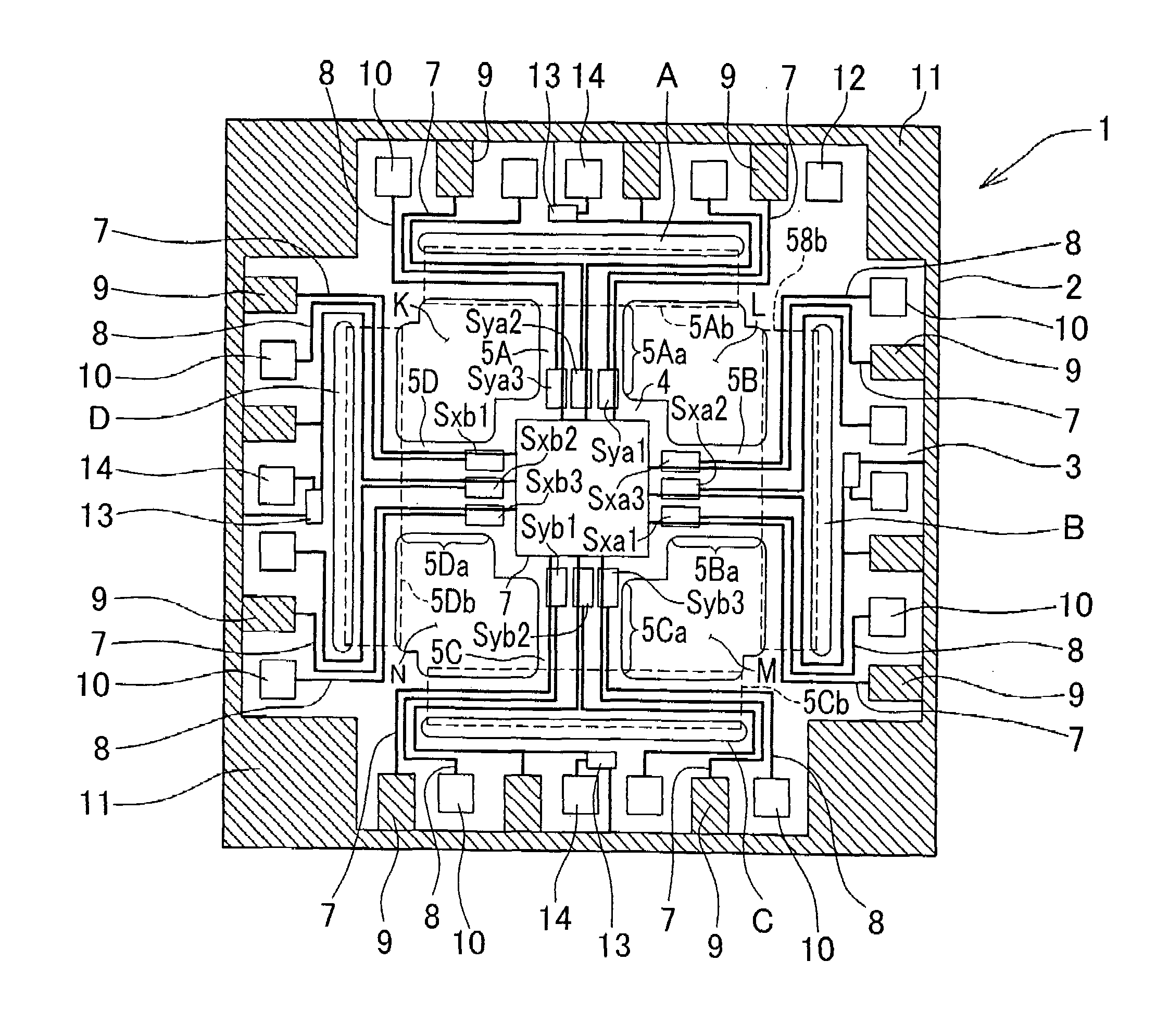
[0089]First, with reference to FIG. 1, a first preferred embodiment of a six-axis force sensor according to the invention will be described. In FIG. 1, the six-axis force sensor chip 1 of this preferred embodiment is formed using a semiconductor substrate 2 which is preferably square in plan shape. The six-axis force sensor chip 1 has a plate-like shape derived from the semiconductor substrate. The six-axis force sensor chip 1 is preferably made by applying semiconductor manufacturing process technology (etching processes such as photolithography, resist patterning, ion implantation, film-forming processes such as P-CVD, sputtering, RIE) to one of its surfaces, to work the plan shape of the square semiconductor substrate itself and to carry out film-forming in predetermined regions of one surface of the semiconductor substrate. In this way, the six-axis force sensor chip 1...


PUM

PropertyMeasurementUnit
radiusaaaaaaaaaa
thicknessaaaaaaaaaa
thicknessaaaaaaaaaa

Abstract

A thin plate-shaped six-axis force sensor chip comprising a semiconductor substrate formed by semiconductor film-forming processes, the sensor chip having through-holes formed therein and arranged so that the sensor chip is functionally divided by the through-holes into an action part to which an external force is applied, a support part to be fixed to an external structure, and a plurality of connecting parts each connecting together the action part and the support part and having a bridge portion of generally T-shaped configuration joined to the action part and an elastic portion joined to the support part. Each of the connecting parts has a plurality of strain resistance devices each comprising an active layer formed on at least one of front and rear faces thereof in an area thereof where deformation strain effectively occurs, the strain resistance devices being electrically connected to corresponding electrodes disposed in the support part.

Description

[0001]This application is a Continuation of Application No. 10 / 339,496, filed on Jan. 10, 2003, now U.S. Pat. No. 6,823,744 and for which priority is claimed under 35 U.S.C. § 120; and this application claims priority of Application No. 2002-005334 filed in Japan on Jan. 11, 2002 and Application No. 2002-059447 filed in Japan on Mar. 5, 2002 under 35 U.S.C. § 119; the entire contents of all are hereby incorporated by reference.FIELD OF THE INVENTION[0002]The present invention relates to a small and highly precise six-axis force sensor chip with strain resistance devices fabricated using semiconductor manufacturing process technology and a six-axis force sensor using such sensor chip.BACKGROUND OF THE INVENTION[0003]Modern automatic machines such as machine tools and robots, in the course of their work or operation, perform work in which they apply forces to workpieces, or are themselves subject to actions of forces from outside. Consequently, it is necessary for machine tools and ro...

Claims


Application Information

Patent Timeline
Patent Type & Authority Patents(United States)
IPC IPC(8): G01L5/16
CPCG01L5/162
Inventor OHSATO, TAKESHIHIRABAYASHI, YUSUKE
Owner HONDA MOTOR CO LTD
Why Eureka
Try Eureka