Nonvolatile semiconductor memory device

A non-volatile, storage device technology, applied in semiconductor devices, information storage, static memory, etc., can solve problems such as wrong writing, failure to flow writing current, and failure to consider changes in source potential

Inactive Publication Date: 2006-09-27
RENESAS TECH CORP
View PDF2 Cites 9 Cited by
  • Summary
  • Abstract
  • Description
  • Claims
  • Application Information

AI Technical Summary

Problems solved by technology

For example, when a large write current flows through the common source line through the memory cell with the lowest resistance value, the potential of the common source line rises, limiting the write current of other memory cells, and causing write malfunctions, etc.
In addition, the writing current becomes large, and due to the resistance of the common source line, a sufficiently large writing current cannot flow, and there is a possibility of erroneous writing.
[0015] In the above-mentioned Patent Document 2, no consideration is given to the fluctuation of the source potential in the common source line at the time of writing and reading.
In addition, it does not consider any changes in the read current / write current corresponding to the location of the selected memory cell.

Method used


Image

  • Nonvolatile semiconductor memory device
  • Nonvolatile semiconductor memory device
  • Nonvolatile semiconductor memory device

Examples


Embodiment approach 1

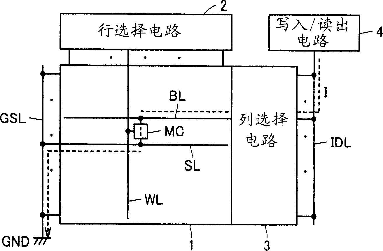
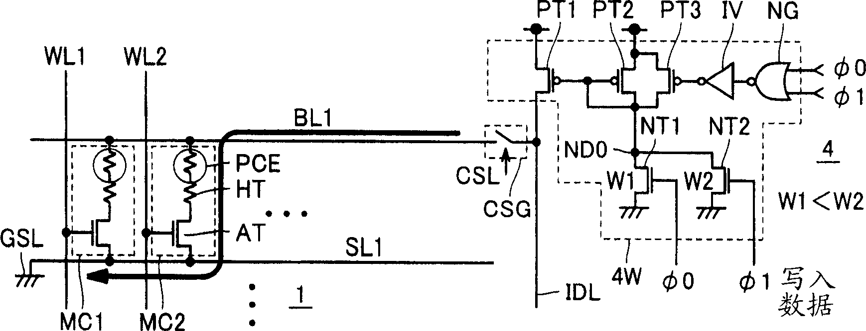
[0098] figure 1 It is a diagram schematically showing the configuration of main parts of the nonvolatile semiconductor memory device according to Embodiment 1 of the present invention. figure 1 In this example, the nonvolatile semiconductor memory device includes a memory cell array 1 in which memory cells MC are arranged in rows and columns. In memory cell array 1 , word lines WL are arranged corresponding to rows of memory cells MC, and bit lines BL are arranged corresponding to columns of memory cells. The source lines SL are arranged corresponding to the bit lines in parallel with the bit lines BL. This source line SL is coupled to a global source line GSL extending along the first side of the memory cell array 1 in a direction perpendicular to the bit line BL and the source line SL. The general source line GSL is coupled to the ground node (ground pad: reference potential source). The memory cell MC, whose structure will be described later, includes a phase-change mate...

change example 1

[0133] Figure 8 It is a diagram schematically showing the configuration of main parts of a nonvolatile semiconductor memory device according to a modified example of Embodiment 1 of the present invention. in the Figure 8 In the shown nonvolatile semiconductor memory device, a sense amplifier 4S is connected in parallel with a variable current source 4W for supplying a write current to an internal data line IDL. Should Figure 8 Other structures of the nonvolatile semiconductor memory device shown are the same as figure 1 and figure 2 The illustrated nonvolatile semiconductor memory devices have the same configuration, and the same reference numerals are assigned to corresponding parts, and detailed description thereof will be omitted.

[0134] The sense amplifier 4S may be a voltage sense type sense amplifier, or may be a current sense type sense amplifier. In the case of the voltage read method, the voltage of the internal data line is compared with a reference voltag...

change example 2

[0143] Figure 10 It is a diagram showing a modified example of the memory cell layout according to Embodiment 1 of the present invention. Figure 10 Here, the bit line BL and the source line SL are respectively composed of a second metal wiring and a first metal wiring, and are arranged in parallel to each other. The first metal wiring and the second metal wiring represent metal wiring on the first layer and metal wiring on the second layer, respectively, in the multilayer wiring structure.

[0144] The word lines WL1-WL4 are arranged at predetermined intervals in a direction crossing the bit line BL. Parallel to the bit line BL, phase change material elements PCE1 and PCE2 are formed close to the word lines WL1 and WL3, respectively. These phase change material elements PCE1 and PCE2 are connected to the bit line BL via contacts CNT11 and CNT12, respectively.

[0145] Contacts CNT21 and CNT22 are formed at positions where contacts CNT11 and CNT12 are point-symmetrical wit...


PUM


Abstract

A path routing from a write current source supplying a write current through an internal data line, a bit line and a source line to a reference potential except a memory cell is configured to have a constant resistance independent of a memory cell position selected in a memory array, and each of the resistance value of the current path between the memory cell and the write current source and the resistance value of the current path between the selected memory cell and the reference potential node is set to 500Omega or lower. A nonvolatile semiconductor memory device having improved reliability of data read/write is achieved.

Description

technical field [0001] The present invention relates to a nonvolatile semiconductor memory device, and more particularly to a structure for improving the reliability of writing / reading data of a phase-change memory which includes a material that selectively changes to a crystalline state (polycrystalline state) according to stored data. state) or amorphous data storage unit. Background technique [0002] Nonvolatile memories that store information in a nonvolatile manner are widely used in applications such as portable devices. This type of non-volatile memory includes, in addition to flash memory that accumulates information by accumulating charge in the floating gate of a multilayer gate transistor, and a variable resistance type that uses the resistance value of the storage element to change according to the stored information. storage unit memory. As such a resistance variable memory, there are known a magnetic memory (MRAM) utilizing the magnetor...

Claims


Application Information

Patent Timeline
Patent Type & Authority Applications(China)
IPC IPC(8): G11C11/56G11C11/15G11C16/04H01L29/792
Inventor 谷崎弘晃日高秀人
Owner RENESAS TECH CORP
Why Eureka
Try Eureka