VCO control circuit and method of operation
Inactive Publication Date: 2005-10-04
RF MAGIC INC
6 Cites 1 Cited by
AI-Extracted Technical Summary
Problems solved by technology
While multiple VCO systems have been used successfully in various systems, some limitations remain in the VCO control circuitry.
One limitation, slow tuning speed, comes as a result of how tuning ranges are selected.
Slow tuning time significantly reduces the performance of a receiver, as channels cannot be changed quickly and receiver tuning can be easily lost.
Slow tuning ...
Benefits of technology
[0009]The present invention now provides systems and methods for a VCO control circuit and method of operation which will enable variability in settling times and faster tuning speeds. In accordance with a first embodiment of the invention, the VCO control circuit includes a variable delay block, a delay counter, and a tuning range selector coupled to one or more tuning circuits, e.g. one or more VCOs, an arrangement of capacitors, varactor diodes, or inductors. The variable delay block receive...
Abstract
A VCO control circuit includes a variable delay block, a delay counter, and a tuning range selector coupled to one or more tuning circuits, e.g. one or more VCOs, an arrangement of capacitors, varactor diodes, or inductors. The variable delay block receives a reference signal and a delay signal for setting the delay amount applied to the reference signal, and in response outputs a delayed reference signal, whereby two or more different delays may be applied to the reference signal. The delay counter receives the delayed reference signal and an outputs a delay counter output signal in response. The tuning range selector receives the delay counter output signal, and changes the tuning range of the one or more connected tuning circuits in response.
Application Domain
Pulse automatic controlOscillations generators
Technology Topic
InductorVaricap +2
Image
Examples
- Experimental program(1)
Example
[0014]For clarity and convenience, features shown in previous figures retain their reference numerals.
DETAILED DESCRIPTION OF SPECIFIC EMBODIMENTS
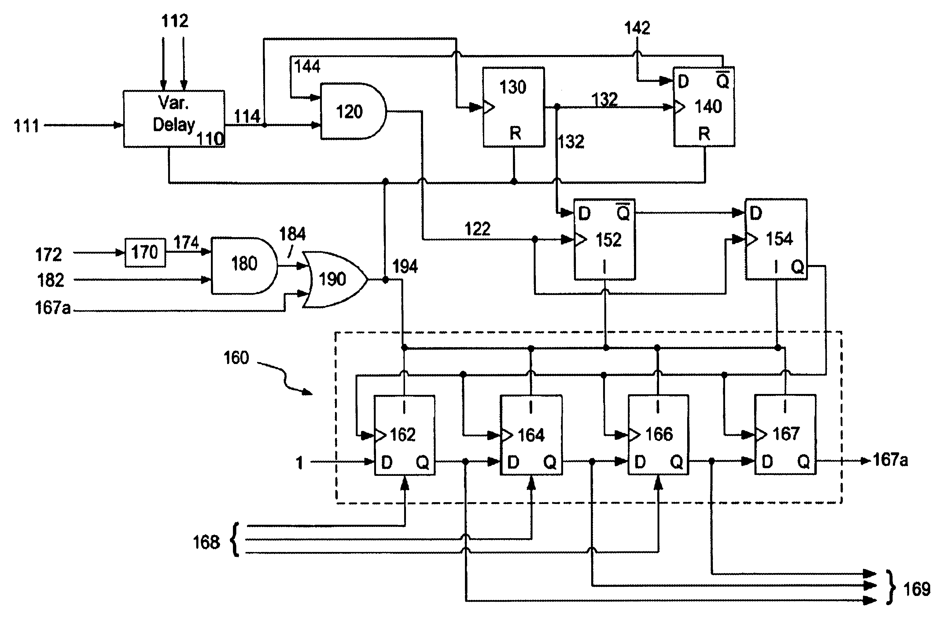
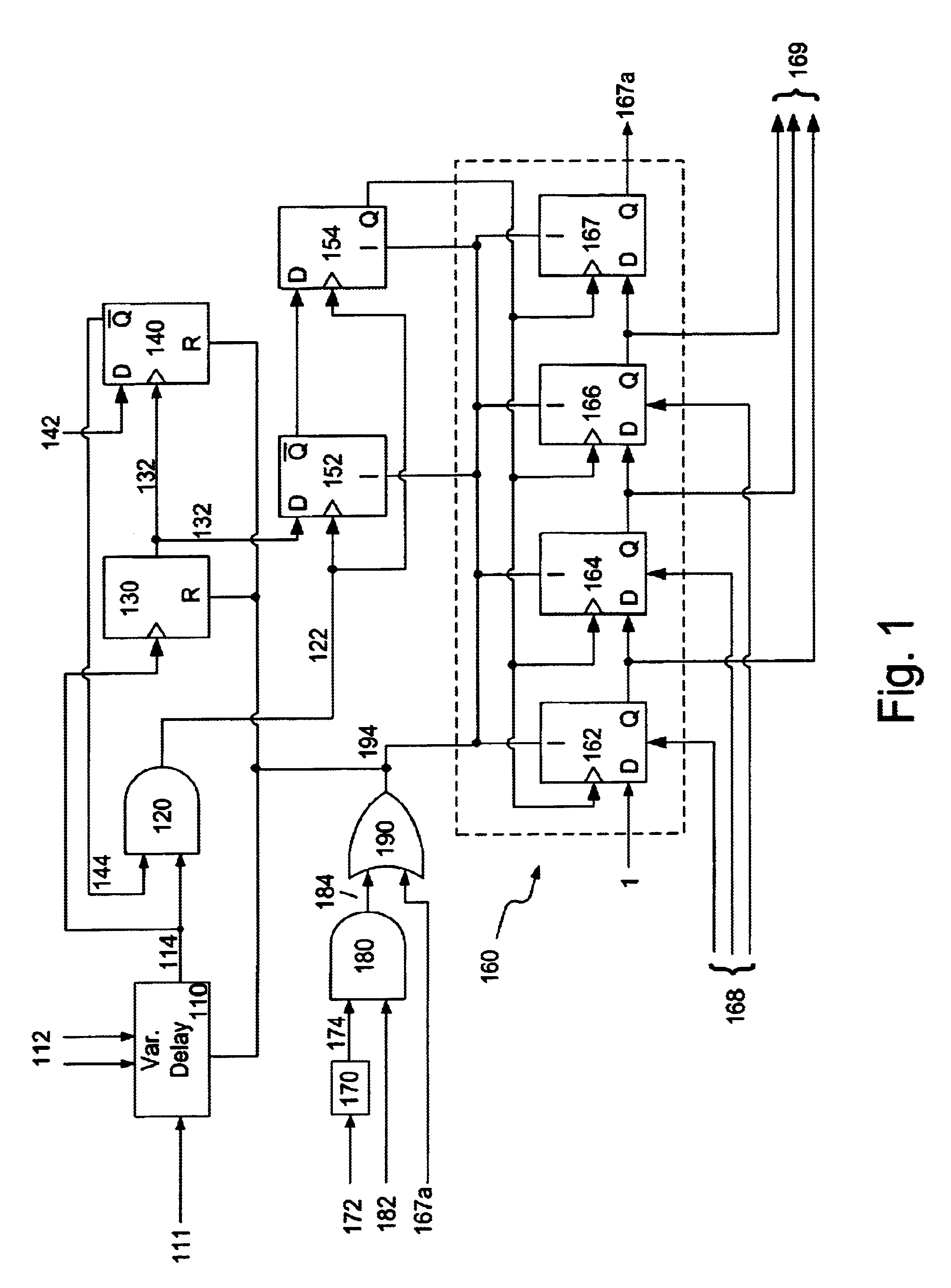
[0015]FIG. 1 illustrates a VCO control circuit 100 in accordance with one embodiment of the present invention. While the following description is presents the tuning circuit as being a VCO, those skilled in the art will appreciate that the tuning circuitry may alternatively be realized as an arrangement of capacitors, varactor diodes, inductors, or a combination of these components. Further, different tuning ranges may be provided by separate VCOs, by one VCO having different tuning ranges, or a combination of both.
[0016]In the illustrated embodiment, the VCO control circuit 100 includes a variable delay block 110, a first AND gate 120, a delay counter 130, lock detect flip-flop 140, flip-flops 152 and 154, a tuning range selector 160 comprising flip flops 162, 164, 166, and 167 collectively configured as a loadable serial shift register 160, logic gate 170, and second AND gate 180, and an OR gate 190. In the preferred embodiment, the aforementioned elements are photolithographically deposited in complementary metal oxide semiconductor (CMOS) material. Of course, other equivalent architectures and/or semiconductor materials may be used in alternative embodiments of the invention
[0017]During operation, a reference signal Fref 111 is coupled to the variable delay block 110. Variable delay block 110 is configured to provide two or more delay values relative to the reference signal Fref 111. In a specific embodiment, three delay values; x1 (no delay), x2, x4, and a “disable” instruction are provided to the delay block 110 via delay set lines 112. An optimal delay time is selected which is sufficient to permit the phase lock loop to “settle” after a particular tuning range is selected, but which is not so long as to delay the lock detection operation. Different delay times may be selected depending upon the chosen reference frequency, as well as other parameters, such as the loop filter response, phase lock loop settling time, and process variation in the circuit fabrication. Delay values other than those mentioned above may be used in alternative embodiments within the present invention.
[0018]When the “disable” delay setting is chosen, the output 114 of the variable delay block 110 is disabled. This process permits tuning range selection through a programming mode, as will be further described below. When one of the other delay settings is chosen, the system operates in an automatic search mode, and a description of this process is now presented.
Automatic Search Mode
[0019]When one of the non-disabled delay settings is chosen, the automatic variable delay block 110 outputs a delayed reference signal dFref 114 to both the AND gate 120 and a delay counter 130. The delay counter 130 is operable to output a pulse after a predefined number of input pulses. In a specific embodiment, the delay counter contains n delay elements and outputs a pulse for every 2n+1 pulses received, although other settings may be chosen in alternative embodiments within the present invention.
[0020]Upon receiving the requisite number of input pulses, the delay counter 130 outputs a clock signal 132 to clock flip-flop 140. Upon clocking, flip-flop 140 in turn outputs a feedback signal 144, the feedback signal 144 being the complement to a lock condition signal 142 provided by a lock detection circuit (not shown). The lock condition signal 142 is the result of a digital lock comparison process.
[0021]In the instance in which the currently selected tuning range results in a locked condition, the feedback signal 144 is in a low state, which disables the output of the first AND gate 120, and thus terminates the tuning range search process. If an unlocked condition is sensed, the feedback signal 144 is high, enabling the output of the first AND gate 120 and thereby permitting the search process to continue.
[0022]In the instance in which the feedback signal 142 is high indicating that a locked condition is not sensed, the first AND gate 120 outputs the delay reference signal dFref 122 as a clock signal to flip-flops 152 and 154. Flip-flip 152 receives the delay counter output 132, and its complementary output is supplied to the data input of flip-flop 154. The output of flip-flop 154 is supplied as clocking signals to serial register flip-flops 162, 164, 166, and 167. Flip-flops 152 and 154 collectively provide the necessary timing to ensure that the clock signal output 122 does not occur before the end of the delay time of the delay counter 130. The output of flip-flop 154 clocks each of the shift register flip-flops 162, 164, 166, and 167 incrementing by one bit the shift register's value after the programmed delay time has elapsed. In the preferred embodiment, the D input port of the flip-flop representing the least significant bit (162 in the illustrated embodiment) is connected to a high state to provide the shift function. Accordingly, the next tuning range is sequentially selected and the circuit begins to count down the program delay time to determine if a high lock signal is received. As described herein, the tuning ranges are provided by tuning circuitry which may consist of VCOs, an arrangement of capacitors, varactor diodes, inductors, and similar components and circuitry. Further, different tuning ranges may be provided by different tuning ranges within one VCO, or a different combination of the aforementioned arrangement of capacitors, varactor diodes, inductors or similar components. The invention is not limited to any specific embodiment of the tuning range circuitry, and any component or circuit which can be used to tune to a predefined frequency may be used in alternative embodiments under the present invention.
[0023]When the highest addressable tuning range has been selected, flip-flop 167 outputs a last tuning range select signal 167A from its Q port, that signal being used as an input to the OR gate 190 to continue the selection process. In this manner, the selection process cycles back to the first tuning range, thereby allowing the circuit to lock if an intermittent condition prevents lock during the first selection cycle. A tuning range select word consisting of the output states of flip-flops 162, 164 and 166 are output on tuning range select lines 169.
[0024]In the preferred embodiment, the search mode is initiated upon receiving a start signal 172. The start signal is provided to a gate 170, which in response produces a start pulse 174. Additionally, a high state search signal 182 is input to the second AND gate 180 along with the start pulse 174. The resulting signal 184 is supplied with the last tuning range select signal 167A to the OR gate 190. The resulting initialization signal 194 initializes flip-flops 162, 164, 166 and 167 and loads the tuning range select word provided by set lines 168. This input word is provided via set lines 168 and used to select the initial tuning range for phase lock.
[0025]In a particular embodiment of the invention, the supplied start signal 172 is also used to initiate other system processes. For example, once the phase locked loop exhibits lock, other initialization pulses may occur which could result in the VCO control circuit switching to another tuning range. Therefore, it is useful to disable the initialization function of the start signal 172 during certain periods. This is accomplished in the illustrated embodiment by applying a low state search signal 182 to the second AND gate. The low state search signal ensures that the initialization signal 184 remains low, and that the flip-flops 162, 164, 166, and 167 remain in their respective states until switched by flip-flop 154.
[0026]In the illustrated embodiment the tuning range selector 160 comprises a shift register made up of flip-flops 162, 164, 166 and 167. In an alternative embodiment, the tuning range selector is replaced with a binary counter operating with an ascending or descending binary counts and decode logic applied subsequently thereafter, although other circuits will be apparent to those skilled in the art. The invention is not limited to any specific tuning range selector, and any circuit operable to control the tuning range within connecting tuning circuitry may be used in alternative embodiments under the present invention.
[0027]Programmed Tuning Mode
[0028]The VCO control circuit 100 may also be used to programmably select a particular tuning range. FIG. 2 illustrates one embodiment of this method in accordance with the present invention. As one of skill in the art will appreciate, the invention is not limited to the particular sequence illustrated, and different embodiments within the invention may include the described processes occurring in a different order.
[0029]At process 202, a “disable” instruction is applied to delay set lines 112 to disable the output variable delay block 110. This results in the clock signal output of the first AND gate 120 to be disabled. At process 204, a high state search signal 182 is applied to the second AND gate 180. At process 206, a tuning range select word is provided to set lines 168. In a particular embodiment, a microcontroller (not shown) programmably provides the tuning range select word via lines 168. At process 208, a start signal 172 is applied to logic gate 170, the gate 170 producing a start pulse 174, which, in combination with the high state search signal 182, produces a high state signal 184, and in turn produces a high state initialization signal 194. The high state of the initialization signal 194 operates to load flip-flops 162, 164, and 166 with the tuning range select word provided on lines 168. The output word consisting of the output states of flip-flops 162, 164 and 166 is provided via tuning range select lines 169 to select the desired tuning range. In a particular embodiment, tuning range select lines 169 are addressably coupled to a plurality of VCOs. In a further specific embodiment, one or more of these VCOs are operable to provide two or more tuning ranges which can be selected by addressing the VCO in a particular manner. Alternatively, the VCOs may comprise only one tuning range, in which case the desired tuning range is selected by addressably selecting the corresponding VCO. Still alternatively, some of the VCOs may provide two or more of the desired tuning ranges and others provide only one tuning range, each being addressable in the manner as described. In an alternative embodiment, the tuning ranges are provided by differing arrangements of capacitors, varactor diodes, inductors, or similar components, the different arrangements of which are addressably selectable.
[0030]At 210, the microcontroller senses the lock condition signal 142, and if a lock condition is detected, the currently selected tuning range provide phase lock, and method terminates. If a locked condition is not detected, the microcontroller programmably provides a second tuning range select word to lines 168, and the aforementioned process repeats. This process may be used to select at least one fewer tuning ranges than are available, the process of which is further described below.
[0031]Tuning Range Selection
[0032]The VCO control circuit and methods described herein can be used to provide many advantages, one of which is the reduction in the number of tuning ranges which need to be selected to ascertain a locked condition. This reduction results in faster phase locked loop settling time and improved receiver performance.
[0033]FIG. 3 illustrates a method for operating the improved VCO control circuit 100 such that one or more tuning ranges can be eliminated from the selection process. A plurality of separate tuning ranges extend (either spaced apart, adjacent, or in an overlapping manner) over a predefined band, the entire plurality of the tuning ranges consisting of a total number. A subset of that total number of tuning ranges is associated with a predefined frequency at 302, the process of which is further described below. In a particular embodiment in which the total number of tuning ranges is three, the subset consists of two tuning ranges, both tuning ranges being associated with the same frequency, for example, 500 MHz. Of course, the present method is applicable in systems employing a different number of tuning ranges, as long as the subset of tuning ranges is at least one fewer than the total number.
[0034]Next at 304, a first of the tuning ranges associated with the predefined frequency is selected from among those within subset, and the tuning circuitry instructed to tune to the predefined frequency within the selected tuning range, described above. The term “first tuning range” is meant to denote the first selected tuning range, not necessarily the lowest or highest tuning range provided thereby. The selection process may be performed as a part of the automatic selection process, or the programmable selection process, each described above. In particular, any method may be used to select a tuning range from the subset of tuning ranges previously identified.
[0035]Subsequently at 306, a determination is made as to whether the selected tuning range results in a locked condition, indicating that the predefined frequency has been tuned to. As described above, the process in one embodiment includes activating the tuning circuit to tune to the predefined frequency, waiting a predetermined settling time and detecting a locked or unlocked condition of the phase locked loop. If a locked condition is not indicated, the process repeats 304 and 306 for another of the tuning ranges within the subset. In the above exemplary embodiment, the third tuning range is selected and its lock condition is checked to determine lock. In this manner, only two of the three VCOs are checked for lock, and accordingly the settling time for the phase locked loop is decreased. In the illustrated embodiment of the control circuit shown in FIG. 1 and in the condition in which tuning range selection of all subset tuning ranges does not result in the detection of lock, the processes 304 and 306 continue repeating times in order to permit the phase lock loop to continue its search for a locked condition when the system experiences a temporary unlocked condition.
[0036]In a particular embodiment of 302, each tuning range is associated with those frequencies over which it potentially extends in all possible conditions. That is, each tuning range is associated with those frequencies that it will produce or tune to under nominal conditions, and under the widest variation of conditions. For example, it may be known that the tuning range of a VCO will vary ±20% due to variations in the fabrication process or operating conditions. As a result of this variation, the tuning range of the VCO may cover its nominal tuning range, cover a lower tuning range, or cover a higher frequency tuning range. Accordingly, the VCO is associated with those lower, nominal, and higher tuning frequencies. Similarly, adjacent VCOs are associated with their lower, nominal and higher tuning frequencies. As a result, some of the tuning frequencies will overlap tuning ranges, especially adjacent tuning range frequencies, and these tuning frequencies will be included in two or more different tuning ranges. The tuning frequencies of at least one of the VCOs, however, will not extend to overlap with these tuning frequencies, and thus at least one tuning range can be eliminated when attempting to tune to the predefined frequency.
[0037]As a particular example of this embodiment, consider a phase lock system consisting of three tuning ranges, each tuning range provided by separate VCOs outputting partially overlapping, but substantially contiguous bands. Variations in the circuit fabrication process, operating temperature, or other effects may tend to shift the VCO output frequency higher or lower in frequency. As a result, a frequency normally output by VCO #1, may after process, temperature, or other variations, result in the VCO #2 outputting that same frequency.
[0038]Assuming in one embodiment that the total variation results in less than a 50% shift in the VCO output frequency, the desired output frequency may be generated by one of two neighboring VCOs which output frequencies nearest to the desired frequency. That is, when the process variation is high, VCO #1 may output the desired frequency, and when the variation is low, VCO #2 may output the desired frequency. Accordingly, two VCOs are associated with each frequency, thereby ensuring that each frequency can be generated over the entire spectrum of temperature and process variation. As described above, a first of the two VCOs may be selected and monitored for lock. If a locked condition is not sensed, the second of the two VCOs is then selected. The third VCO is removed from the selection and lock monitoring process for this particular frequency, and the PLL settling time is reduced by one third.
[0039]The foregoing description has been presented for purposes of illustration and description. It is not intended to be exhaustive or to limit the invention to the precise form disclosed, and obviously many modifications and variations are possible in light of the above teaching. The described embodiments were chosen in order to best explain the principles of the invention and its practical application to thereby enable others skilled in the art to best utilize the invention in various embodiments and with various modifications as are suited to the particular use contemplated. It is intended that the scope of the invention be defined by the claims appended hereto.
PUM


Description & Claims & Application Information
We can also present the details of the Description, Claims and Application information to help users get a comprehensive understanding of the technical details of the patent, such as background art, summary of invention, brief description of drawings, description of embodiments, and other original content. On the other hand, users can also determine the specific scope of protection of the technology through the list of claims; as well as understand the changes in the life cycle of the technology with the presentation of the patent timeline. Login to view more.