Device for thermal treatment of substrates

a technology for thermal treatment and substrates, applied in lighting and heating apparatus, charge manipulation, furnaces, etc., can solve the problems of increasing pressure forces between support tips and wafers, unusable particles, and mechanical impressions of support elements in wafers, so as to prevent the crazing of support elements on the wafer surface and hold the height or position of substrates essentially in the chamber

Inactive Publication Date: 2005-10-11
MATTSON TECHNOLOGY +1
View PDF15 Cites 23 Cited by
  • Summary
  • Abstract
  • Description
  • Claims
  • Application Information

AI Technical Summary

Benefits of technology

[0009]Pursuant to the invention, this object is realized in that the support elements are movable essentially parallel to the plane of the substrate. Due to the movable configuration of the support elements, they can follow a movement of the wafer during an expansion as a consequence of the thermal treatment. Thus, a scraping of the support elements upon the wafer surface is prevented. Instead of an elongated scratch, the support elements cause only a point-type impression. Furthermore, due to the movement that is directed essentially parallel to the substrate, the height or position of the substrates within the chamber is held essentially constant.

Problems solved by technology

Unfortunately, these support tips have the drawback that they break off easily and thereby result in undesired particles.
Furthermore, the support tips leave behind mechanical impressions in the wafer that rests upon them, since at high temperatures the wafer material is relatively soft.
Especially with wafers having relatively large diameters, such as, for example, 300 mm wafers, which have a weight of 130 g instead of 50 g for wafers having a 200 mm diameter, the pressure forces between support tips and wafer increase and thus the problem of mechanical impressions increases.
With this method, a double break produced by elastic deformation is measured that results with many transparent and isotropic materials due to deformation.
The mechanical impressions and scratches, as well as inhomogeneity of the wafer temperature during the thermal treatment, lead to dislocation errors, so-called slip lines, in the crystalline structure of the semiconductor wafer.
Although these occur on the underside, i.e. the support side of the wafer, during the thermal treatment of the wafer they can, if the thermal stress is sufficiently great, propagate to the upper surface and damage or adversely affect the structures that are disposed on the upper surface.
As already mentioned, due to the contact with the support pins, however, there results a localized cooling off of the wafer in the region of the contact, which leads to inhomogeneity of the temperature distribution upon the wafer.
This problem was solved in the past in that the contact surface between support pin and wafer was kept small, which, however, worsened the aforementioned problem of scratching.
However, this edge support results in the problem that during the thermal treatment the wafer sags, which again enhances the formation of dislocation errors or slip lines.
However, with these holding pins the aforementioned problems of scratching occur that result from a relative movement between substrate and pin as a consequence of thermal expansion of the substrate.

Method used


Image

  • Device for thermal treatment of substrates
  • Device for thermal treatment of substrates
  • Device for thermal treatment of substrates

Examples


first embodiment

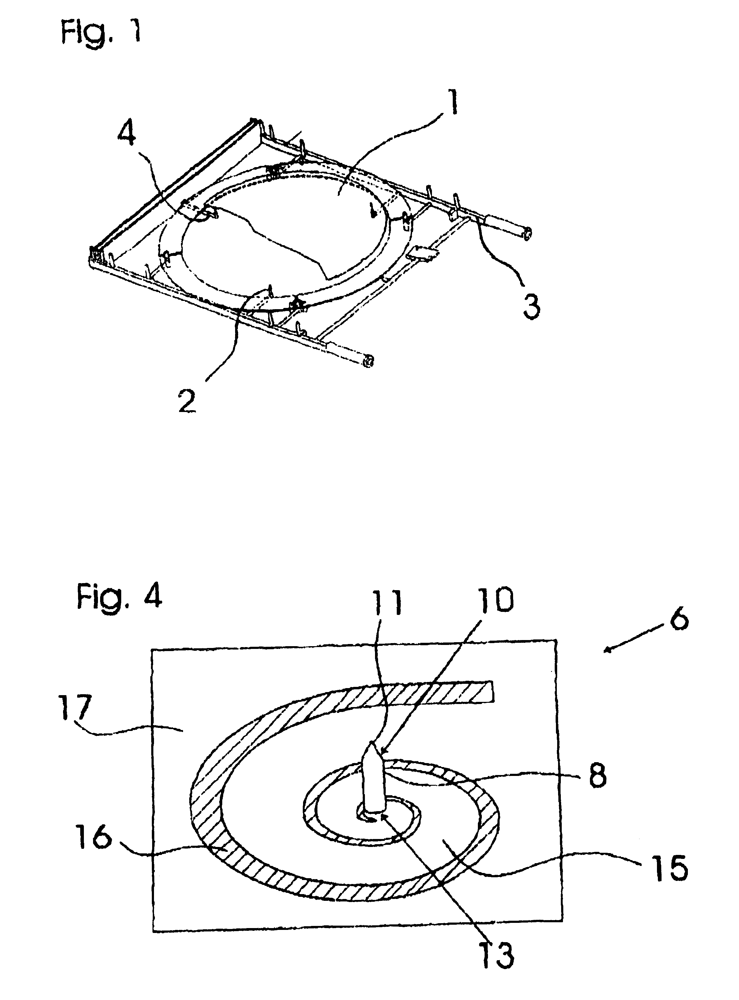
[0043]FIG. 4 shows a carrier construction 6 for a support element 8 in the form of a support pin. The support pin 8 has a first end 10 with a support tip 11 for receiving a semiconductor wafer. An opposite end 13 of the support pin 8 is secured in a suitable manner to a flat helical spring 15. The helical spring 15 is formed by cutting out a portion 16 from a thin plate 17, for example a thin quartz plate. Due to the cutout portion 16 in the quartz plate 17, the flat helical spring 15 is resilient not only in a horizontal direction but also in a vertical direction.

second embodiment

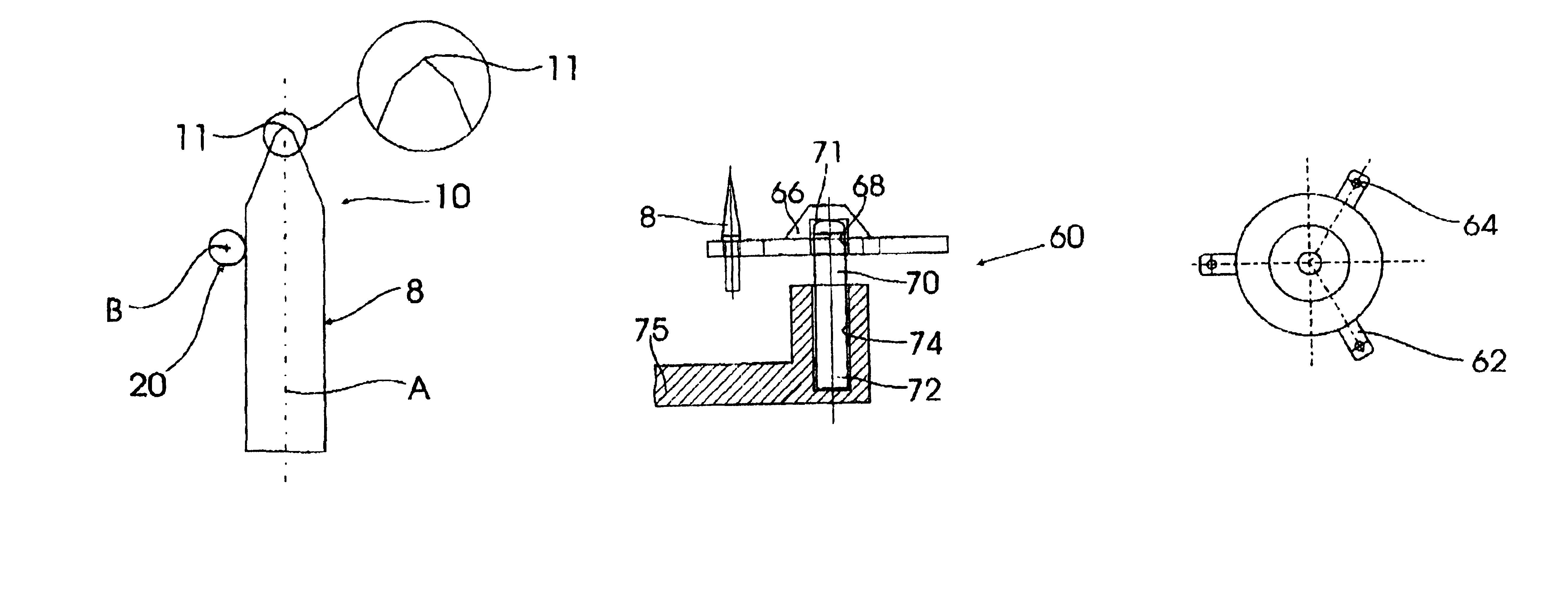
[0044]FIGS. 5 and 6 show the present invention for a movable suspension of a support pin 8. The support pin 8 has a first end 10 on which is formed a support tip 11. In this connection, the end 10 of the support pin 8 is embodied as a double cone. The support tip 11 is formed by one cone having an opening angle between 50 degrees and 130 degrees, and preferably between 80 degrees and 100 degrees. Following this cone is a second cone having an opening or generating angle between 5 and 45 degrees and preferably between 5 and 25 degrees. The thus-formed support tip is sturdy and reduces the danger that the tip will break off.

[0045]The support pin 8 has a longitudinal axis A. Mounted on one side of the support pin 8 is a pivot pin 20 having a longitudinal axis B. The longitudinal axis B of the pivot pin 20 extends perpendicular to the longitudinal axis A of the support pin 8, and is laterally offset relative thereto.

[0046]The pivot pin 20 is received in a suitable holding device, such a...


PUM


Abstract

The aim of the invention is to reduce the formation of scratches in a device for the thermal treatment of substrates, in particular, semiconductor substrates, in a chamber in which the substrate is placed upon support elements. According to the invention, said aim is achieved by means of displaceable support elements.

Description

BACKGROUND OF THE INVENTION[0001]The present invention is related to an apparatus for the thermal treatment of substrates, especially semiconductor substrates, in a chamber in which the substrates are placed upon support elements.[0002]An apparatus of this type for the treatment of substrates is known, for example, from DE-A-198 21 007 of the same applicant. With this apparatus, the support elements for carrying semiconductor wafers are rigidly connected to a rotary plate that is rotated for the homogenization of the thermal treatment of a semiconductor wafer.[0003]An alternative carrier construction for the apparatus of the aforementioned type is illustrated, for example, in FIG. 1. Here a wafer 1 is placed upon conically shaped support studs 2 which are also called pins. The pins, along with their holding means 4, are rigidly secured to a carrier frame 3. The pins have conically shaped support tips in order to keep the contact surfaces between the support elements and the wafer sm...

Claims


Application Information

Patent Timeline
Patent Type & Authority Patents(United States)
IPC IPC(8): H01L21/67H01L21/687H01L21/00H01L21/683H01L21/324
CPCH01L21/67115H01L21/68742H01L21/6875H01L21/68785H01L21/324
Inventor KREISER, UWEWEBER, KARSTENLERCH, WILFRIEDGRANDY, MICHAELSCHMID, PATRICKNIESS, JURGENALTUG, OLGUN
Owner MATTSON TECHNOLOGY
Why Eureka
Try Eureka