Semiconductor light emitting device including photonic band gap material and luminescent material

a technology of light-emitting devices and photonic band gaps, which is applied in the direction of semiconductor devices, basic electric elements, electrical equipment, etc., can solve the problems of difficult and expensive fabrication of dbr b>30/b> with thickness control required, and the filter does not have well-behaved transmittance and reflectance characteristics,

Active Publication Date: 2005-10-18
LUMILEDS
View PDF7 Cites 111 Cited by
  • Summary
  • Abstract
  • Description
  • Claims
  • Application Information

AI Technical Summary

Problems solved by technology

LED is that the SWP filter does not have well-behaved transmittance and reflectance characteristics to efficiently transmit and reflect the primary light and the secondary light over a range of angles, respectively.
The SWP filter exhibits a strong angular dependency, and the large range of incident angles results in undesirable transmittance and reflectance characteristics.
There are s...

Method used


Image

  • Semiconductor light emitting device including photonic band gap material and luminescent material
  • Semiconductor light emitting device including photonic band gap material and luminescent material
  • Semiconductor light emitting device including photonic band gap material and luminescent material

Examples


Embodiment Construction

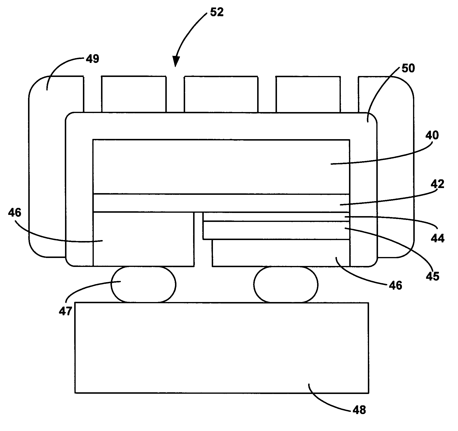
[0019]FIG. 3 illustrates a light emitting structure according to embodiments of the invention. A flip chip semiconductor light emitting device includes a substrate 40, an n-type region 42, and active, light emitting region 44, and a p-type region 45. Contacts 46 connect to the p- and n-type regions and electrically and physically connect the device to a mount 48 via interconnections 47.

[0020]A luminescent material layer 49 is disposed over the light emitting device. Luminescent material layer 49 is any suitable material capable of absorbing light emitted by active region 44 and converting that light to light of a different wavelength. Usually, luminescent layer 49 includes a phosphor material as the luminescent material, though other luminescent materials such as organic dyes may be used. Luminescent material layer 49 may include more than one luminescent material, as well as other materials that are not luminescent. Luminescent material layer 49 may include one or more phosphors de...


PUM


Abstract

A light emitting structure includes a semiconductor light emitting device capable of emitting first light having a first peak wavelength, a luminescent material capable of emitting second light having a second peak wavelength disposed over the semiconductor light emitting device, and a photonic band gap material disposed between the light emitting device and the luminescent material. The photonic band gap material is capable of transmitting the first light and reflecting the second light, regardless of the angle of incidence of the first and second light.

Description

BACKGROUND[0001]1. Field of Invention[0002]The present invention relates to semiconductor light emitting devices with a photonic band gap material disposed between the device and a luminescent material layer.[0003]2. Description of Related Art[0004]Semiconductor light emitting devices such as light emitting diodes (LEDs) are among the most efficient light sources currently available. Material systems currently of interest in the manufacture of high brightness LEDs capable of operation across the visible spectrum include group III–V semiconductors, particularly binary, ternary, and quaternary alloys of gallium, aluminum, indium, and nitrogen, also referred to as III-nitride materials; and binary, ternary, and quaternary alloys of gallium, aluminum, indium, and phosphorus, also referred to as III-phosphide materials. Often III-nitride devices are epitaxially grown on sapphire, silicon carbide, or III-nitride substrates and III-phosphide devices are epitaxially grown on gallium arsenid...

Claims


Application Information

Patent Timeline
IPC IPC(8): H01L33/00H01L33/44H01L33/50H01L33/58
CPCH01L33/50H01L33/44H01L33/504H01L33/508H01L2933/0083
Inventor STOCKMAN, STEPHEN A.
Owner LUMILEDS
Why Eureka
Try Eureka