Micro-cantilever type probe card

a micro-cantilever and probe card technology, applied in the field of probe cards, can solve the problems of not easy to control the location, electric wiring, and the replacement of all the probes, and achieve the effects of preventing the deformation of the planarity of the probe due to the bending characteristics of the circuit board, reducing maintenance costs, and easy to make electric wiring

Inactive Publication Date: 2005-10-18
AMST CO LTD
View PDF13 Cites 19 Cited by
  • Summary
  • Abstract
  • Description
  • Claims
  • Application Information

AI Technical Summary

Benefits of technology

[0014]Therefore, the object of the present invention is to provide a probe card wherein multiple probes positioned very closely and firmly together while the probe's location and whole planarity are controlled, and wherein the electric wiring is easily made.
[0015]Another object of the present invention is to provide a probe card wherein the degrading of the probe's planarity due to the bending characteristics of the circuit board is prevented, and the repairing of the malfunctioning probe is enabled and the maintenance cost lowered.
[0017]Another object of the present invention is to provide a probe card wherein even if some of the probes became defective while measuring the device's characteristics, it would be possible to replace the defective part, thus, reducing the cost.
[0026]Preferably, at least a capacitor may be provided on the printed circuit to decrease the electric noise.

Problems solved by technology

However, in the known probe card, it is not easy to control the location, the planarity, and the electric wiring.
Further, because all the probes are provided on the same circuit board as a set, it is inevitable to replace all of the probes if some of the probes become defective.
Further, because a separate circuit board is used between the probes and the main circuit board, the bending characteristics of the circuit board causes degrading of the probe's planarity, and also causes increase of the manufacturing costs of the probe card.
Further, when the required test area of the device is too large to manufacture, it is impossible to manufacture a proper probe card with good planarity.
Moreover, if defects appear on some of the probes while using the probe card for the measurement of the device's characteristics, the whole circuit board had to be replaced, causing increase in the maintenance cost.

Method used


Image

  • Micro-cantilever type probe card
  • Micro-cantilever type probe card
  • Micro-cantilever type probe card

Examples


Embodiment Construction

[0040]Reference will now be made in detail to the present invention as illustrated in the accompanying drawings.

[0041]FIG. 4 is a plane figure of the probe card applied to the probe card structure of the present invention. FIG. 5 is a cross sectional view of the probe card along the line B—B in FIG. 4, FIG. 6 illustrates a disassembled probe card of FIG. 4.

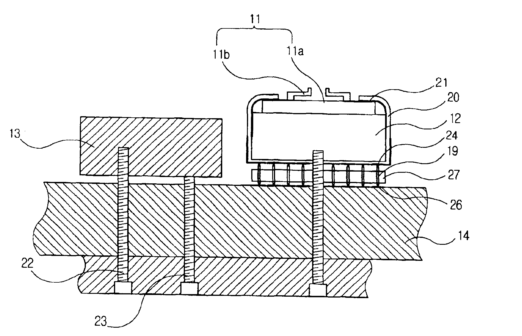
[0042]Referring to FIGS. 4, 5 and 6, in the probe card (10) of the present invention, the probe sections (11) are fixed on the linear supporting structures (12) by adhesives (not illustrated). The supporting structures (12) are fixed on the rectangular frame shaped fixing structures (13) having a rectangular shaped hole. The fixing structure (13) is fixed on the center of the upper surface of the circular circuit board (14). A reinforcing plate (18) is installed on the lower surface of the circuit board (14). As illustrated in FIG. 8, the probe sections (11) and the circuit board (14) are electrically connected by the pogo pin (19...


PUM


Abstract

A probe card has probe sections with silicon probes formed on an insulated circuit board that are connected by an adhesive on the supporting structures. The supporting structures are supported by fixing structures with each of the fixing structures being fixed on the circuit board. The probe card has the probe section's wiring and the circuit board's wiring being electrically connected by a metallic wiring and the sub printed circuit and the pogo pin electrically connected by an anisotropic conducting film with the sub printed circuit board and the pogo pin. A metallic layer is formed by the plating of the probe in the probe section. This reduces the manufacturing costs by enabling the damaged probes during manufacturing to be discarded and the others being used continually.

Description

BACKGROUND OF THE INVENTION[0001]1. Field of the Invention[0002]The present invention relates to a probe card to inspect the electric properties of the micro electronic device. More particularly, the present invention relates to a probe card structure wherein, when the probes fabricated by etching the silicon substrate are mounted on the main circuit board, the assembly characteristics and the convenience of circuit connection are improved.[0003]2. Description of the Related Art[0004]Generally, during or after manufacturing an electrical circuit device such as a semiconductor integrated circuit device, or before attaching the lead frame to the device, the device should be inspected whether the device was manufactured according to the specifications, and whether the measured whole or partial electric properties coincides with the desirable electric properties for the designed device. The inspection device used to inspect the device is the probe station. A probe card is one of the mai...

Claims


Application Information

Patent Timeline
Patent Type & Authority Patents(United States)
IPC IPC(8): G01R1/073G01R1/067
CPCG01R1/07342G01R1/06733
Inventor KIM, DONG ILSONG, BYUNG CHANGJEONG, HA POONG
Owner AMST CO LTD
Why Eureka
Try Eureka