System and method for specifying integrated circuit probe locations

a technology of integrated circuits and probe locations, applied in the field of integrated circuit design, can solve the problems of difficult to rearrange congested areas of integrated circuits to make room for probe locations, many nodes of integrated circuits may be affected by unnecessary delay, and only being able to access electronic components of the chip from the backsid

Inactive Publication Date: 2005-10-18
GLOBALFOUNDRIES INC
View PDF13 Cites 11 Cited by
  • Summary
  • Abstract
  • Description
  • Claims
  • Application Information

AI Technical Summary

Benefits of technology

[0011]A method for including probe locations in an integrated circuit may include specifying one or more probe cells in a netlist. The netlist represents a functional design for an integrated circuit. The method may further include mapping the netlist into a physical layout design for the integrated circuit. The physical layout design includes one or more probe locations for one or more nodes of the integrated circuit as specified in the netlist. The integrated circuit may be fabricated according to the physical layout design so that the fabricated integrated circuit includes the one or more backside probe locations. The integrated circuit may be fabricated at least partially on the frontside of a semiconductor substrate. The one or more probe locations of the integrated circuit provide an electrical contact to probe one or more corresponding nodes of the integrated circuit from a frontside or backside of the semiconductor substrate. The integrated circuit may be tested by measuring one or more characteristics of the integrated circuit by probing the one or more probe locations from either the frontside or backside of the semiconductor substrate, depending on whether frontside or backside (or both) types of probe cells were included in the design.
[0012]The one or more probe cells may be specified in the netlist by indicating a location of each of one or more of the probe cells in a functional description of the integrated circuit, such as an HDL description. The netlist may be generated from the functional description. In another embodiment, an existing netlist may be edited to include the probe cells on specified nets.
[0013]In one embodiment, one or more integrated circuit design tools may be operable to generate a description representing a design for an integrated circuit. The description may specify one or more probe locations for one or more nodes of the integrated circuit. The one or more design tools may be operable to map the description to a physical layout design for the integrated circuit. The physical layout design may include one or more probe locations for one or more nodes of the integrated circuit as specified in the description. The physical layout design provides information for fabricating the integrated circuit to include the one or more probe locations according to the physical layout design. The one or more design tools may be stored in a memory of a computer system and be executable by one or more processors of the computer system.

Problems solved by technology

The corresponding numbers of required I / O pads and device package terminals have increased as well, as have the design and testing complexities of the chips, device packages and PCBs.
When a chip fails or when testing of the chip is performed, access to electronic components of the chip may only be possible from the backside of the device.
However, it may be difficult to rearrange congested areas of the integrated circuit to make room for probe locations.
In addition, if probe locations are added for every node, unnecessary delay may be added to many nodes of the integrated circuit.

Method used


Image

  • System and method for specifying integrated circuit probe locations
  • System and method for specifying integrated circuit probe locations
  • System and method for specifying integrated circuit probe locations

Examples


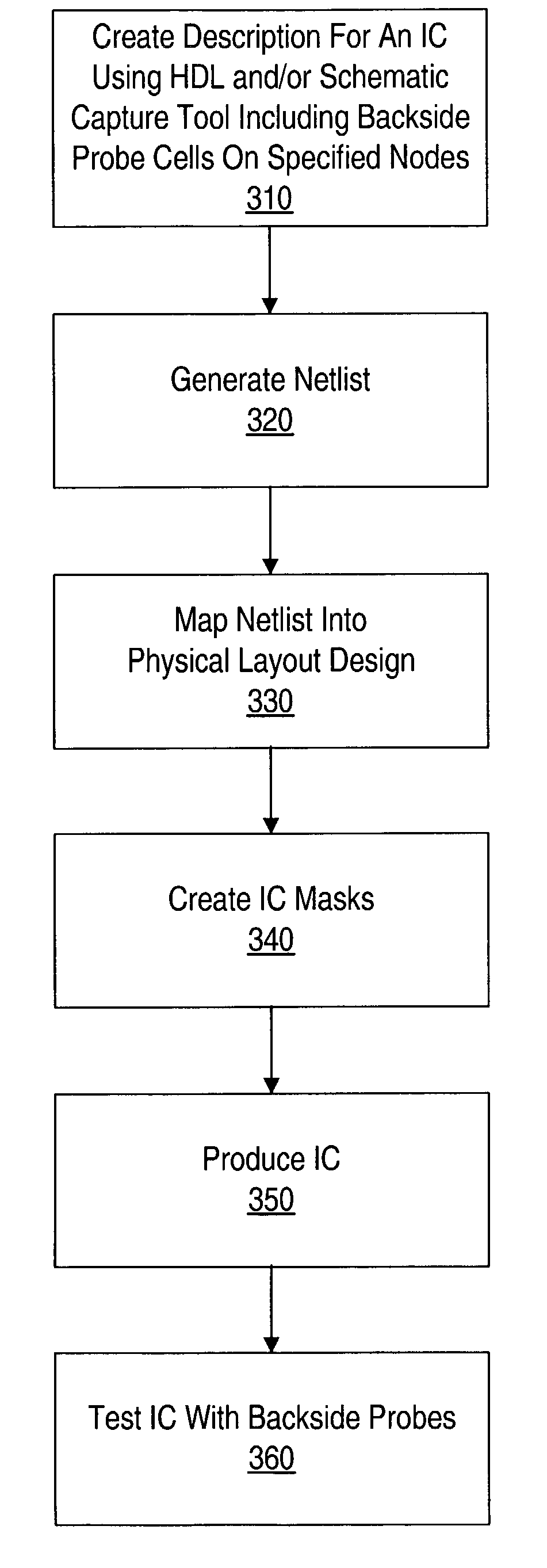
Embodiment Construction

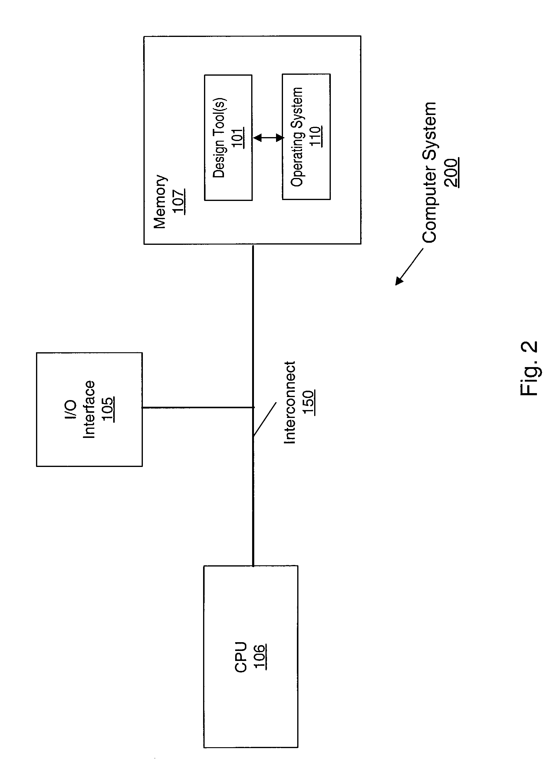
[0022]FIG. 2 illustrates a computer system 200 that may execute design tool(s) 101 for including probe cells within an integrated circuit design, according to one embodiment. Computer system 200 may include components such as memory 107, at least one central processing unit (CPU) or processor 106, an input / output (I / O) interface 105, operating system 110 and device interconnect 150. Computer system 200 may further include other software and hardware components, and interconnect 150 for moving data from one component to another. Interconnect 150 may be a point-to-point interconnect, a shared bus, a combination of point-to-point interconnects and one or more buses, and / or a bus hierarchy including a system bus, CPU bus, memory bus and I / O buses such as peripheral component interconnect (PCI), universal serial bus (USB), and accelerated graphics port (AGP). Although not shown, an interconnect or bus controller, such as a bus bridge, may connect the interconnect 150 to various component...


PUM


Abstract

A method for including probe locations in an integrated circuit may include specifying probe cells prior to the place and route stage of the design process. The probe cell locations may be specified in a functional description of the integrated circuit, such as an HDL description from which a netlist may be generated. Alternatively, an existing netlist may be edited to include the probe cells on specified nets. The probe locations are included in the physical layout design along with the rest of the integrated circuit components during place and route. The integrated circuit may be fabricated according to the physical layout design so that the fabricated integrated circuit includes the one or more probe locations.

Description

BACKGROUND[0001]1. Field of the Invention[0002]This invention relates to design of integrated circuits, and more particularly to inclusion of probe cells in an integrated circuit design for probing of the integrated circuit.[0003]2. Description of the Related Art[0004]During manufacture of an integrated circuit (e.g., a microprocessor), electronic components are formed upon and within a frontside surface of a semiconductor substrate having opposed frontside and backside surfaces. The electronic components are connected together by electrically conductive interconnect lines referred to as signal lines, forming an electronic circuit. Signal lines, for connecting to external devices, may be terminated at flat metal contact regions called input / output (I / O) pads. Following manufacture, the integrated circuit, also referred to as chip, is typically secured within a protective semiconductor device package (e.g., carrier). Each I / O pad of the chip is then connected to one or more terminals...

Claims


Application Information

Patent Timeline
Patent Type & Authority Patents(United States)
IPC IPC(8): G06F17/50G01R31/317G01R31/319
CPCG01R31/31722G01R31/31723G01R31/31905G06F17/5022G06F17/5068G06F30/39G06F30/33G06F30/3308
Inventor MCKEONE, TOMLOYER, BRUCE A.
Owner GLOBALFOUNDRIES INC
Why Eureka
Try Eureka