Methods of fabricating crossbar array microelectronic electrochemical cells

a technology of electrochemical cells and crossbar arrays, applied in the field of microelectronic devices, can solve the problems of molecule located in the gap between the first and second set of metal lines to be damaged or destroyed

Inactive Publication Date: 2005-10-25
NORTH CAROLINA STATE UNIV
View PDF10 Cites 13 Cited by
  • Summary
  • Abstract
  • Description
  • Claims
  • Application Information

AI Technical Summary

Problems solved by technology

This fabrication process may cause the molecules located in the gap between the first and second set of metal lines to be damaged or destroyed during the deposition and patterning of the second set of metal lines.

Method used


Image

  • Methods of fabricating crossbar array microelectronic electrochemical cells
  • Methods of fabricating crossbar array microelectronic electrochemical cells
  • Methods of fabricating crossbar array microelectronic electrochemical cells

Examples


Embodiment Construction

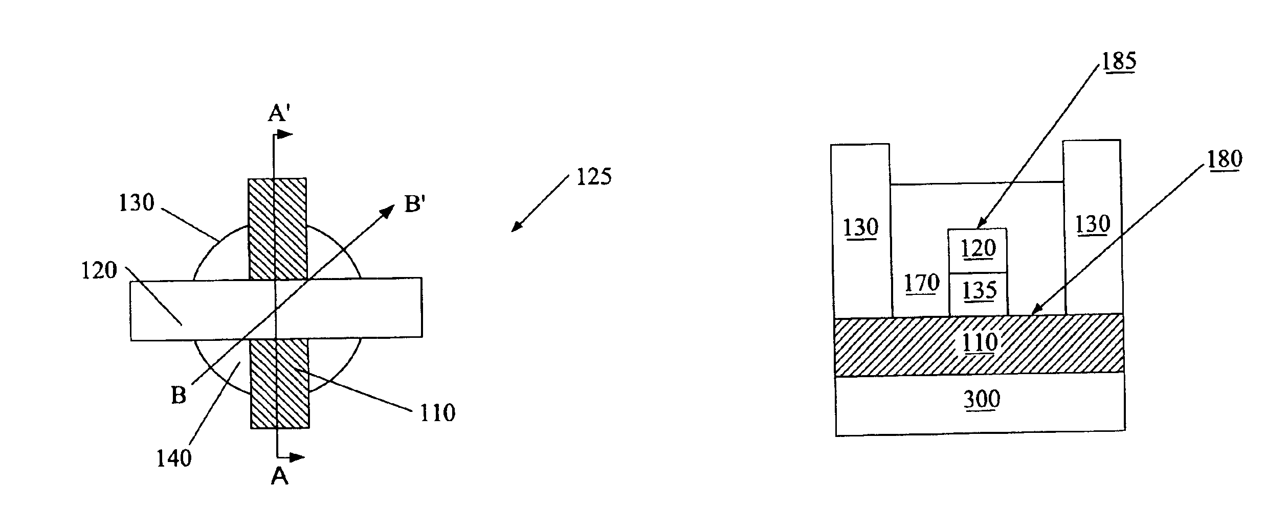
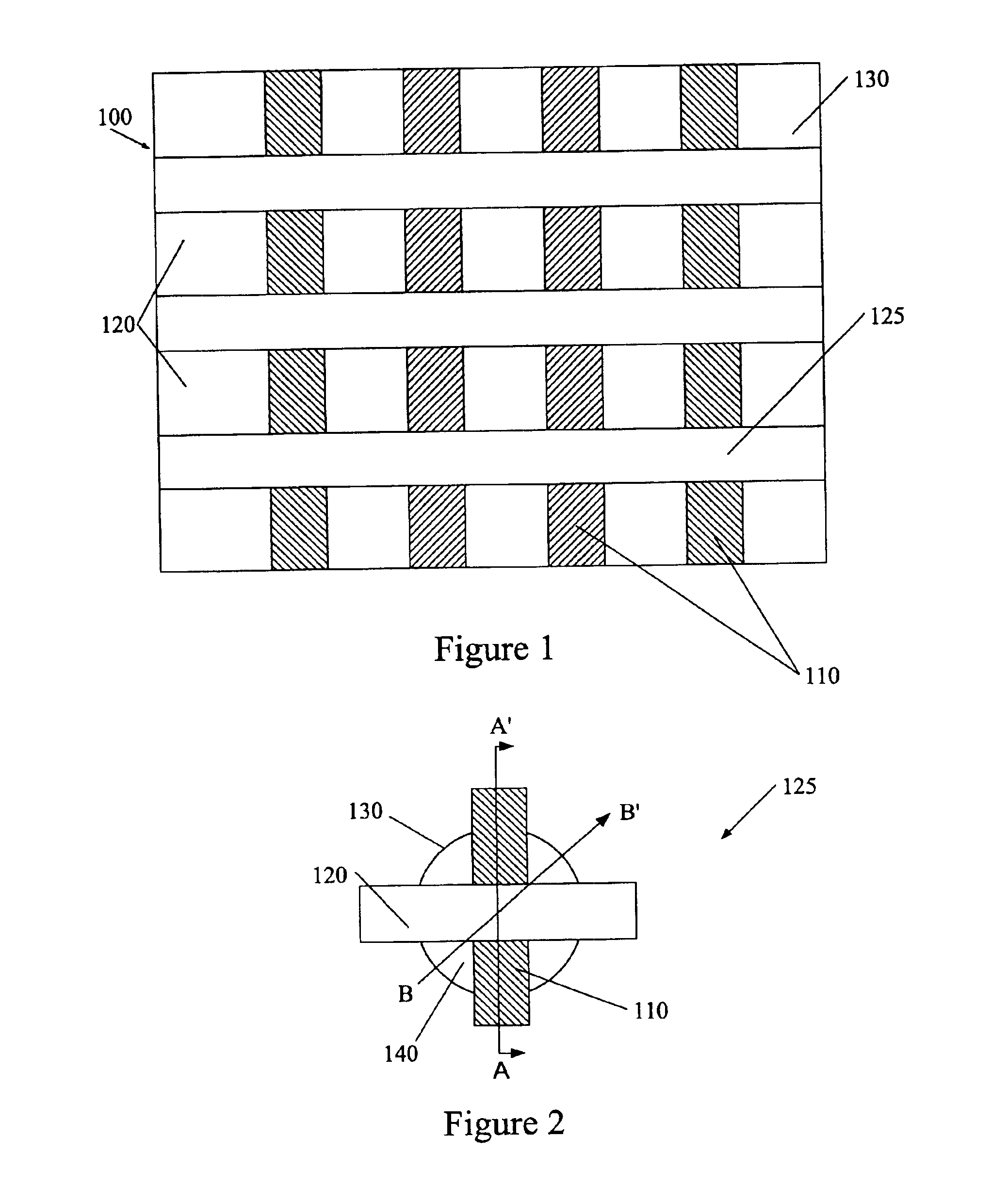
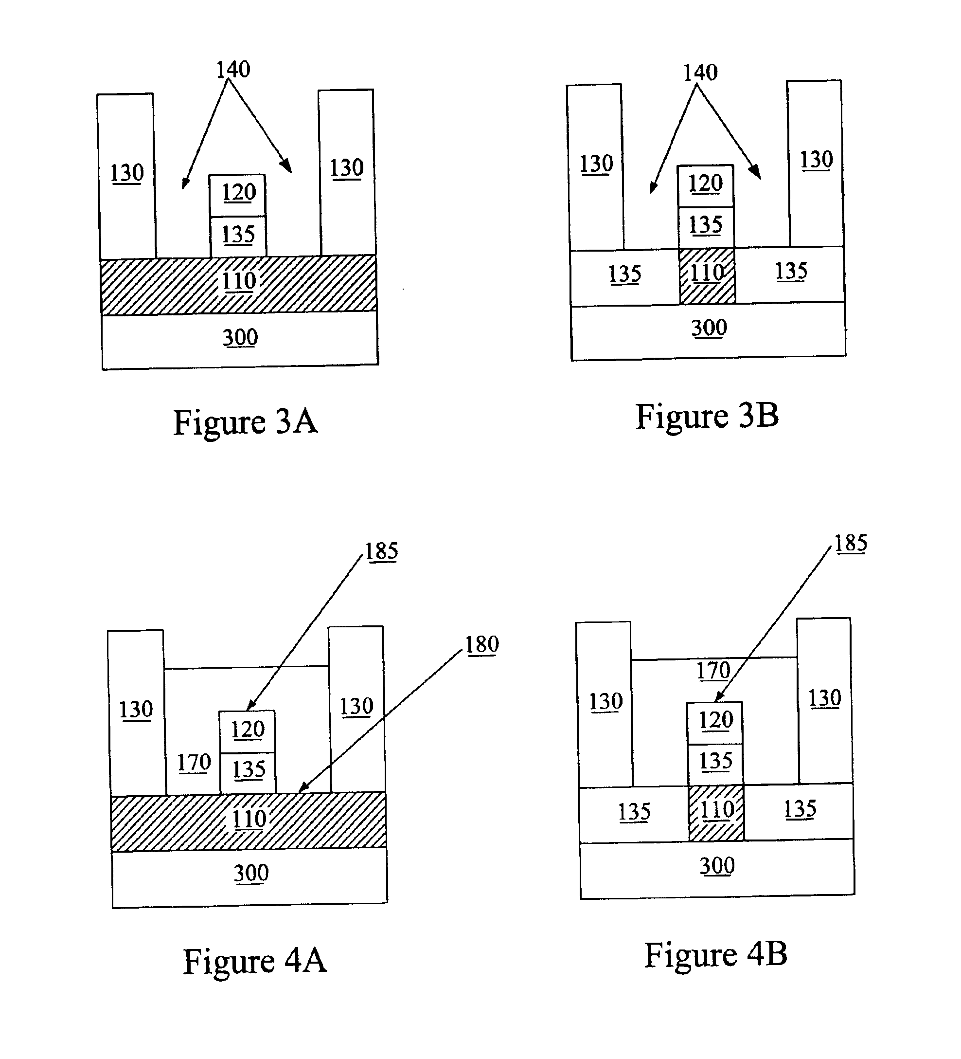
[0024]The present invention will now be described with reference to the FIGS. 1 through 12, which illustrate various embodiments of the present invention. As illustrated in the Figures, the sizes of layers or regions are exaggerated for illustrative purposes and, thus, are provided to illustrate the general structures of the present invention. Furthermore, various aspects of the present invention are described with reference to a layer being formed on a substrate or other layer. As will be appreciated by those of skill in the art, references to a layer being formed on another layer or substrate contemplates that additional layers may intervene. References to a layer being formed on another layer or substrate without an intervening layer are described herein as being formed “directly” on the layer or substrate. Like numbers refer to like elements throughout.

[0025]As described in detail below, microelectronic electrochemical cell structures according to some embodiments of the present...


PUM

PropertyMeasurementUnit
temperaturesaaaaaaaaaa
molecular weightaaaaaaaaaa

Abstract

The present invention provides microelectronic electrochemical structures and related fabrication methods. A composite microelectronic structure is provided that includes first and second conductors dielectrically isolated from one another at a crossing thereof, the crossing surrounded by a dielectric material. A portion of the dielectric material around the crossing of the first and second conductors is removed to form a well that exposes respective outer surfaces of the first and second conductors and a molecule is deposited in the well such that the deposited molecule contacts the exposed outer surfaces of the first and second conductors.

Description

RELATED APPLICATION[0001]This application is related to and claims priority from U.S. Provisional Application Ser. No. 60 / 433,923, filed Dec. 17, 2002, entitled Crossbar Array Microelectronic Electrochemical Cells and Fabrication Methods Therefor, the disclosure of which is hereby incorporated herein by reference as if set forth in its entirety.FIELD OF THE INVENTION[0002]The present invention relates to microelectronic devices and, more particularly, to microelectronic electrochemical devices and fabrication methods therefor.BACKGROUND OF THE INVENTION[0003]Recently, there has been a great interest in the field of molecular electronics. The potential for molecular memory devices has been studied where charge storage can be used to read and / or write data. Detailed information with respect to this topic can be found in the following publications: Harell, S. et al., Microelectron Eng., 30, 11 (1996); Reed, M. A. et al., Since, Volume 278, 252-254 (1997); Reed, M. A., Proc. IEEE, Volum...

Claims


Application Information

Patent Timeline
Patent Type & Authority Patents(United States)
IPC IPC(8): G11C13/02
CPCB82Y10/00G11C13/0014G11C13/0016G11C13/02Y10T29/49108G11C2213/77Y10T29/49115Y02P70/50
Inventor MISRA, VEENADAMIANO, JR., JOHN
Owner NORTH CAROLINA STATE UNIV
Why Eureka
Try Eureka