Bipolar transistor test structure with lateral test probe pads

a bipolar transistor and probe pad technology, applied in semiconductor/solid-state device testing/measurement, semiconductor device details, semiconductor/solid-state device testing/measurement, etc., can solve the problems of cost and expense in both processing time and expense, and achieve the effect of not incurring the cost and time necessary

Inactive Publication Date: 2005-10-25
TELEDYNE SCI & IMAGING
View PDF5 Cites 13 Cited by
  • Summary
  • Abstract
  • Description
  • Claims
  • Application Information

AI Technical Summary

Benefits of technology

[0008]The present invention seeks to provide a novel test transistor structure and associated characterization method that allows transistor characterization to be completed before the wafer has been fully fabricated, and in particular before the upper metallization is laid down. The invention is particularly applicable to HBTs, and permits bad wafers to be identified and discarded without incurring the cost and time necessary to fabricate the upper metallization.

Problems solved by technology

This is costly in terms of both processing time and expense.

Method used


Image

  • Bipolar transistor test structure with lateral test probe pads
  • Bipolar transistor test structure with lateral test probe pads
  • Bipolar transistor test structure with lateral test probe pads

Examples


Embodiment Construction

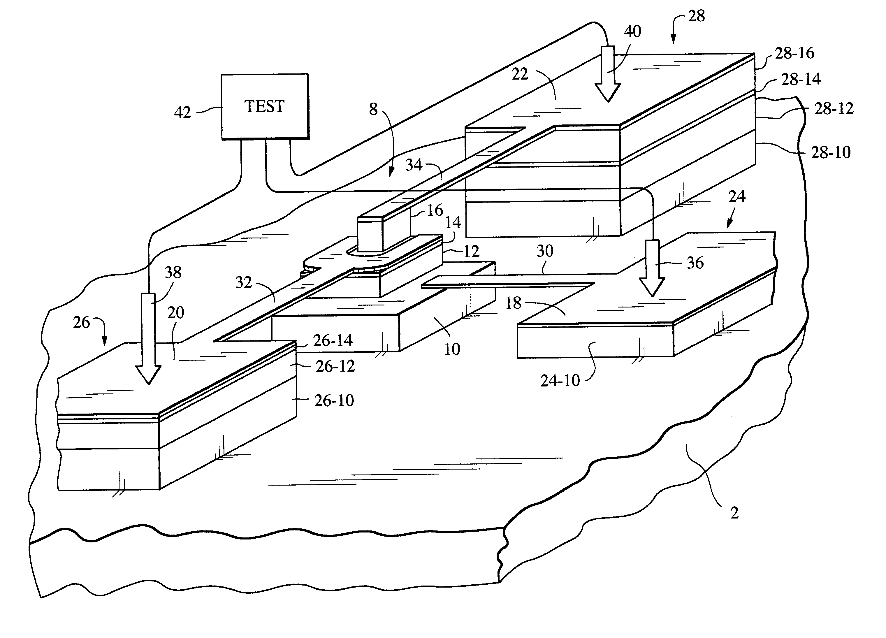
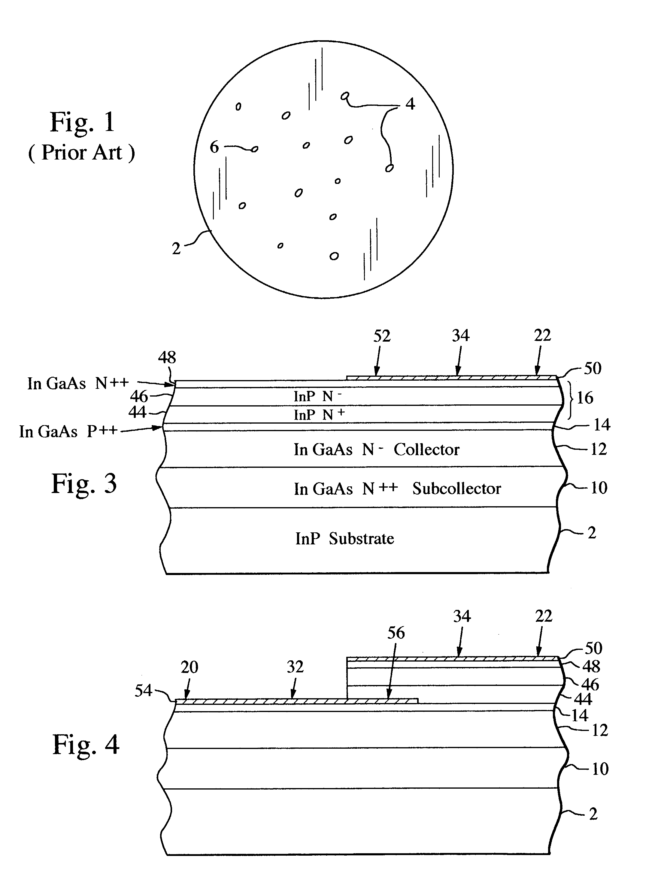
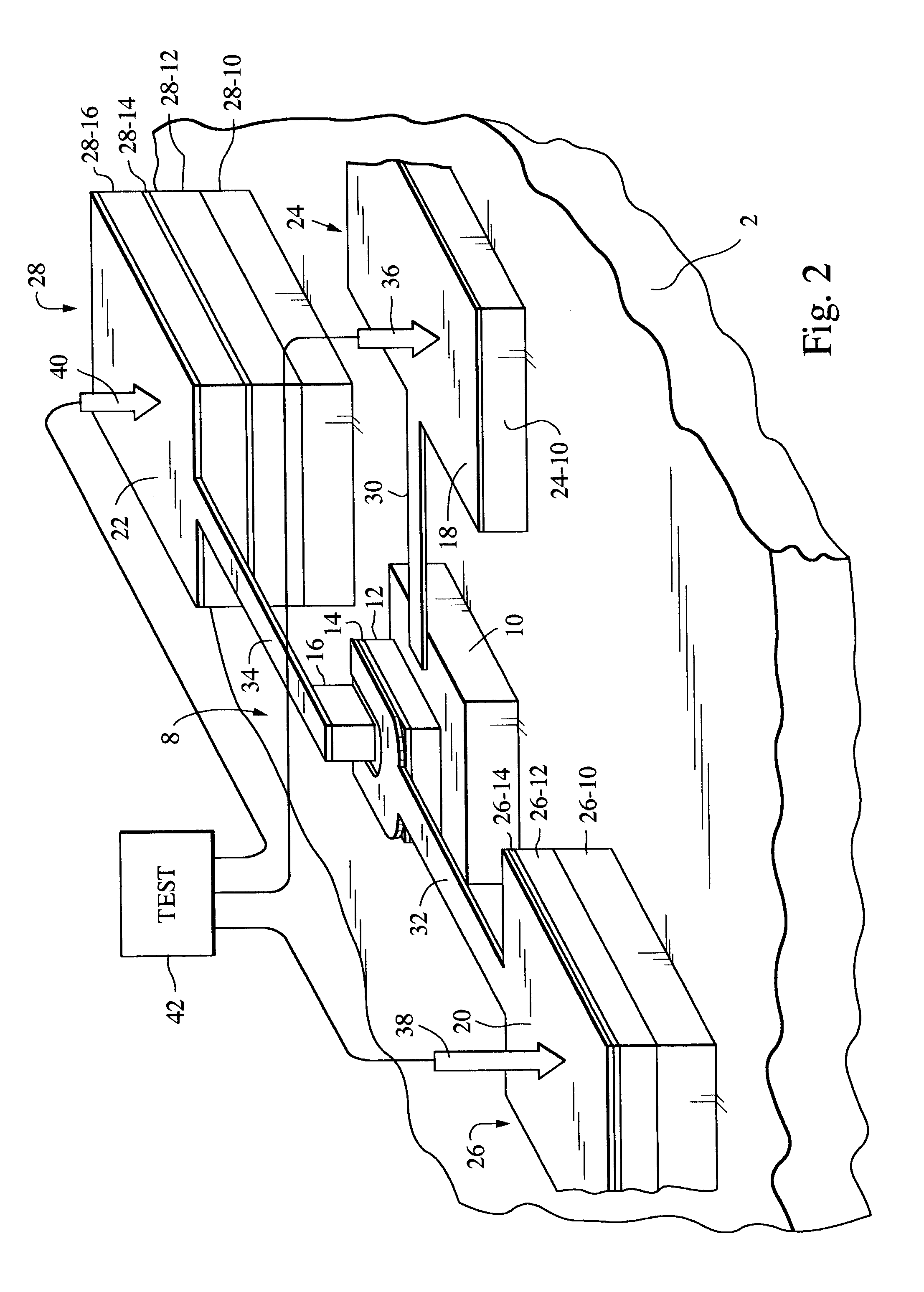
[0017]FIG. 1 illustrates in very simplified form a semiconductor wafer 2 that bears an array of bipolar transistors. Some of the transistors are test devices 4 which are provided only for purposes of characterizing all of the transistors on the wafer, and are not included in the functional operation of the wafer's circuitry. The remaining transistors, illustrated by reference number 6, are referred to herein as circuit transistors because they play an active role in the operation of the wafer's circuitry. The test transistors are much fewer in number than the circuit transistors, and are scattered around the wafer so that possible variations in transistor quality at different locations of the wafer can be detected. The transistors can be organized into an overall wafer-sized circuit, or the wafer can be diced into separate IC chips with their own respective circuits in which case the test transistors would normally be provided between chip areas. Lead wires and other circuit element...


PUM


Abstract

Test probe pads are located lateral to, and spaced from, the emitter, base or collector region of a bipolar transistor, preferably on separate pedestals, and connected to their respective transistor regions by air bridges. The probe pads, transistor contacts and air bridges are preferably formed as common metallizations. In the case of an HBT, a gap in the subcollector below the air bridges insulates the test transistor from capacitor loading by the probe pads. The test transistors can be used to characterize both themselves and functional circuit transistors fabricated with the same process on the same wafer by testing at an intermediate stage of manufacture, thus allowing wafers to be discarded without completing the manufacture if their transistors do not meet specifications.

Description

RELATED APPLICATION[0001]This application is a continuation of Ser. No. 10 / 075,758 by the same inventors, filed Feb. 14, 2002 now U.S. Pat. No. 6,605,825.BACKGROUND OF THE INVENTION[0002]1. Field of the Invention[0003]This invention relates to the characterization of bipolar transistors, and more particularly to a novel heterojunction bipolar transistor (HBT) test structure and method in which test probe pads are provided lateral to respective transistor regions prior to forming an upper metallization.[0004]2. Description of the Related Art[0005]In characterizing newly manufactured bipolar transistors to determine whether they operate properly and meet specifications, a small portion of the transistors on a wafer (typically less than one percent) are dedicated as test devices. Since all of the transistors on the wafer are fabricated in a common process, they will generally exhibit common operating characteristics. Therefore, characterizing the relatively few test transistors can be ...

Claims


Application Information

Patent Timeline
Patent Type & Authority Patents(United States)
IPC IPC(8): H01L23/544
CPCH01L22/34H01L2924/0002H01L2924/00
Inventor BRAR, BERINDER P. S.LI, JAMES CHINGWEIHIGGINS, JOHN A.
Owner TELEDYNE SCI & IMAGING
Why Eureka
Try Eureka