
Nonvolatile semiconductor memory device capable of realizing optimized erasing operation in a memory array

a memory array and non-volatile technology, applied in the field of semiconductor memory devices, can solve the problems of inability to apply configuration, inability to perform normal rewriting, and inability to increase the voltage of depleted memory cells to 0v or higher, so as to achieve the effect of improving the erasing rate and speed of erasing operation

Inactive Publication Date: 2005-10-25
RENESAS ELECTRONICS CORP
View PDF8 Cites 23 Cited by
  • Summary
  • Abstract
  • Description
  • Claims
  • Application Information

AI Technical Summary

Benefits of technology

The invention provides a nonvolatile semiconductor memory device with a memory array that includes a plurality of word lines, a plurality of bit lines, and a plurality of memory cells each connected to a corresponding word line and a corresponding bit line. The erasing operation of the device has the following characteristics: 1. An erasing mode that allows for independent erasing of different pages in a time sharing manner, reducing the number of erasure verification determinations. 2. A rewriting process that is performed continuously on different pages, preventing errors caused by fluctuations in threshold voltage. 3. A multi-page erasing mode that improves the erasing rate by simultaneously erasing pages in different blocks. 4. A configuration where page addresses are set to be continuous in multiple banks, increasing the erase unit and improving the erasing rate. 5. A selective erasure verification determination process that minimizes the number of erasure verification determinations. Overall, the invention provides a more efficient and effective erasing operation for nonvolatile semiconductor memory devices.

Problems solved by technology

Specifically, when the unit of writing is one page, the unit of erasing is two pages.(2) The AG-AND type of the hot electron injecting writing method has a problem such that, if there is a depleted bit in a string, rewriting cannot be performed normally.
Specifically, when a plurality of depleted memory cells (over-erased cells: threshold voltage of 0V or less) exist on the same bit line in a block, even if one of the depleted cells is selected and the threshold voltage is increased again to 0V or higher, current flows in the other depleted cells so that the threshold voltage of the depleted memory cell cannot be increased to 0V or higher.(3) The “one sense latch circuit+two SRAMs” configuration has a problem such that the sequence of the “one sense latch circuit+two data latch circuits” configuration cannot be applied.

Method used


Image

  • Nonvolatile semiconductor memory device capable of realizing optimized erasing operation in a memory array
  • Nonvolatile semiconductor memory device capable of realizing optimized erasing operation in a memory array
  • Nonvolatile semiconductor memory device capable of realizing optimized erasing operation in a memory array

Examples


Embodiment Construction

[0055]Embodiments of the invention will be described in detail hereinbelow with reference to the drawings. In all of the diagrams for explaining the embodiments, the same reference numerals are designated to members having the same functions and their repetitive description will not be given.

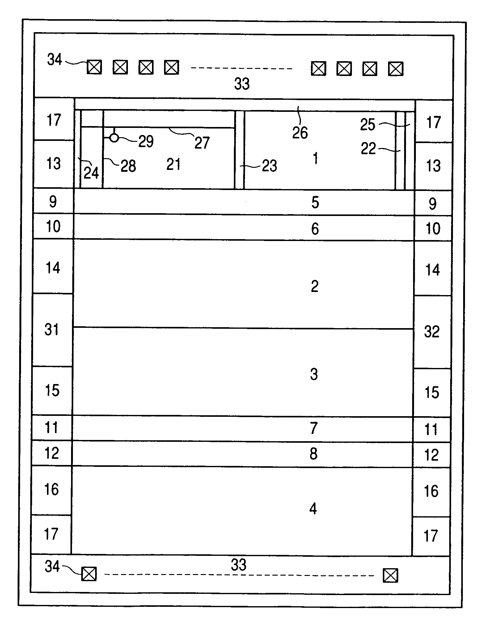
[0056]An example of the configuration of a flash memory as an embodiment of a nonvolatile semiconductor memory device of the invention will be described with reference to FIG. 1.

[0057]The flash memory of the embodiment is, although not limited, as an example, a flash memory capable of storing data of a plurality of bits as threshold voltages in each of memory cells and constructed by a plurality of banks which can operate independently of each other. The flash memory includes four banks 1 to 4, sense latch columns 5 to 8 corresponding to the banks 1 to 4, Y-direct circuits 9 to 12, SRAMs 13 to 16, and indirect circuits 17. Circuit elements constructing those circuits are formed on a single semic...


PUM


Abstract

A nonvolatile semiconductor memory device capable of realizing optimized erasing operation in a memory array configuration in which a plurality of pages correspond to and are connected to each of a plurality of word lines and higher speed of the erasing operation. In a flash memory, the erasing operation is performed by an erasing method of erasing a plurality of pages arbitrarily selected in a lump. In a two-page erasing mode, page erasure, page pre-erasure verification, page rewriting process, page pre-rewriting verification, and page upper end determining process are performed in order. The method realizes, particularly, (1) suppression of the number of erase verification times to the minimum by performing erase verification only on arbitrary one even-numbered or odd-numbered page in the pages to be erased in consideration of variations in the erasing characteristic, and (2) prevention of erroneous determination of the upper end of erasure since it is unnecessary to set a memory cell to be rewritten every rewrite verification by continuously executing the rewriting process page by page.

Description

TECHNICAL FIELD[0001]The present invention relates to a semiconductor memory device and, more particularly, to a technique effective when applied to erasing operation of a nonvolatile semiconductor memory device such as a multi-value flash memory having a memory array of a configuration in which a plurality of blocks are constructed every plural word lines and a plurality of pages are connected to each of the plurality of word lines.BACKGROUND ART[0002]The inventors herein have examined a flash memory as an example of a nonvolatile semiconductor memory device as follows.[0003]For example, in a flash memory, a nonvolatile memory element having a control gate and a floating gate is used as a memory cell, and a memory cell can be constructed by a single transistor. For such a flash memory, the concept of a so-called “multi-value” flash memory for storing data of two or more bits per memory cell in order to increase storage capacity has been proposed. In such a multi-value flash memory,...

Claims


Application Information

Patent Timeline
Patent Type & Authority Patents(United States)
IPC IPC(8): G11C16/06G11C16/34G11C16/24G11C16/04
CPCG11C16/16G11C16/24G11C16/3436G11C16/344G11C16/3445G11C16/3459G11C16/0433G11C2216/18
Inventor TAKASE, YOSHINORIKURATA, HIDEAKIYOSHIDA, KEIICHIMATSUBARA, KENKANAMITSU, MICHITAROYUASA, SHINJI
Owner RENESAS ELECTRONICS CORP
Learn More