Structure and method for fabrication of a leadless chip carrier

a chip carrier and fabrication method technology, applied in the direction of semiconductor devices, semiconductor/solid-state device details, electrical equipment, etc., can solve the problems of large number of holes drilling, and small device details, and achieve low parasitics, low cost and time, and efficient heat dissipation

Inactive Publication Date: 2005-11-01
SKYWORKS SOLUTIONS INC
View PDF35 Cites 33 Cited by
  • Summary
  • Abstract
  • Description
  • Claims
  • Application Information

AI Technical Summary

Benefits of technology

[0017]As described in the detailed description herein, the present invention's structure provides efficient dissipation of heat generated by the semiconductor die, while also providing low parasitics, and a low inductance and resistance ground connection.

Problems solved by technology

The requirement of smaller, more complex, and faster devices has resulted in new challenges not only in the fabrication of the die itself but also in the manufacturing of various packages, structures, or carriers that are used to house the die and provide electrical connection to “off-chip” devices.
Moreover, the cost and time associated with the manufacturing of the discrete semiconductor package and the cost and time associated with drilling a large number of holes in the printed circuit board are among additional reasons why alternatives such as surface mount devices and chip carriers have gained popularity.
For example, conventional chip carriers still introduce too much parasitics and still do not provide a low inductance and resistance ground connection to the die.
Conventional chip carriers also have a very limited heat dissipation capability and suffer from the concomitant reliability problems resulting from poor heat dissipation.
The resulting thermal stresses can cause cracking or a separation of the die from the chip carrier and, as such, can result in electrical and mechanical failures.

Method used


Image

  • Structure and method for fabrication of a leadless chip carrier
  • Structure and method for fabrication of a leadless chip carrier
  • Structure and method for fabrication of a leadless chip carrier

Examples


Embodiment Construction

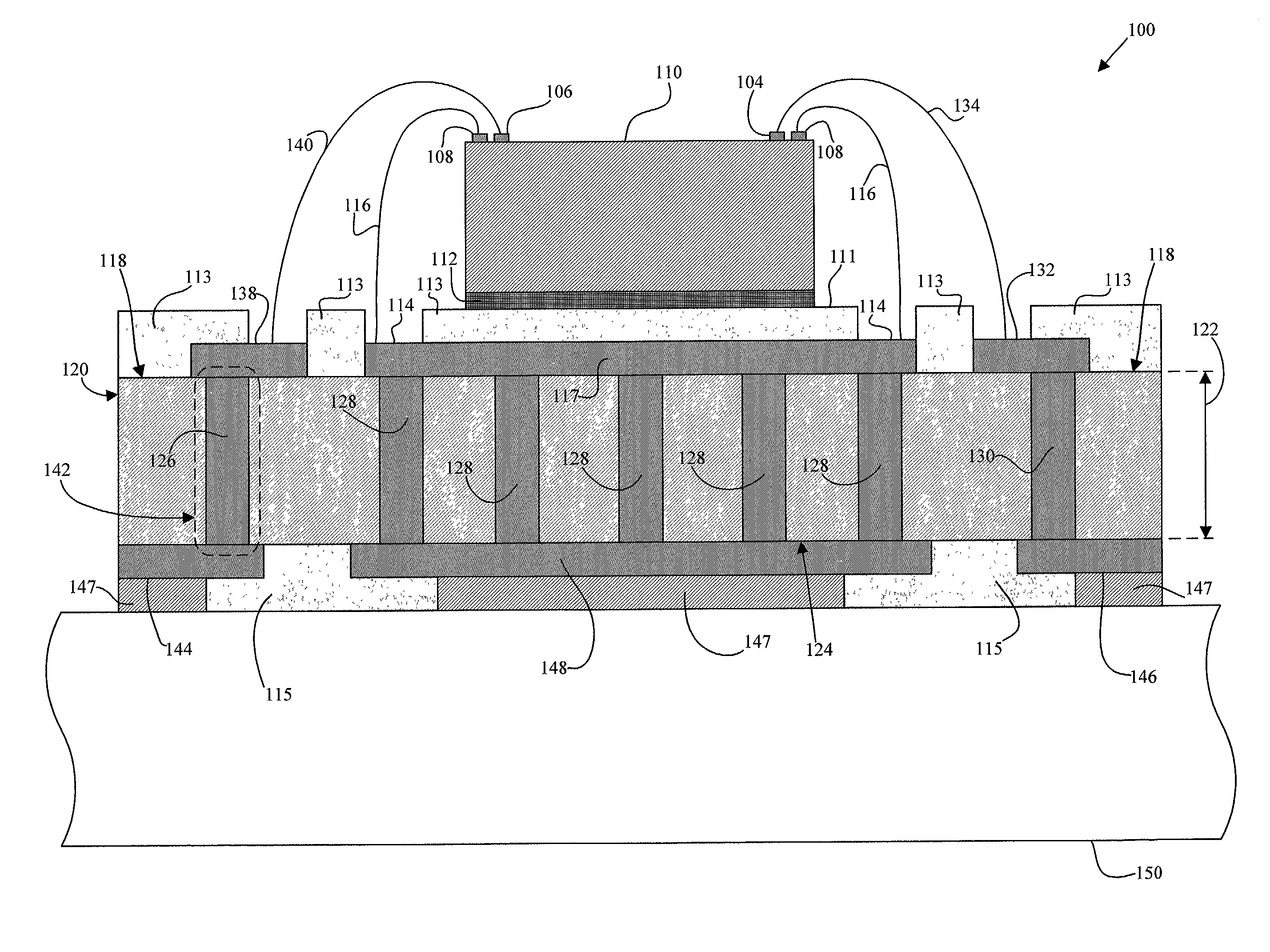
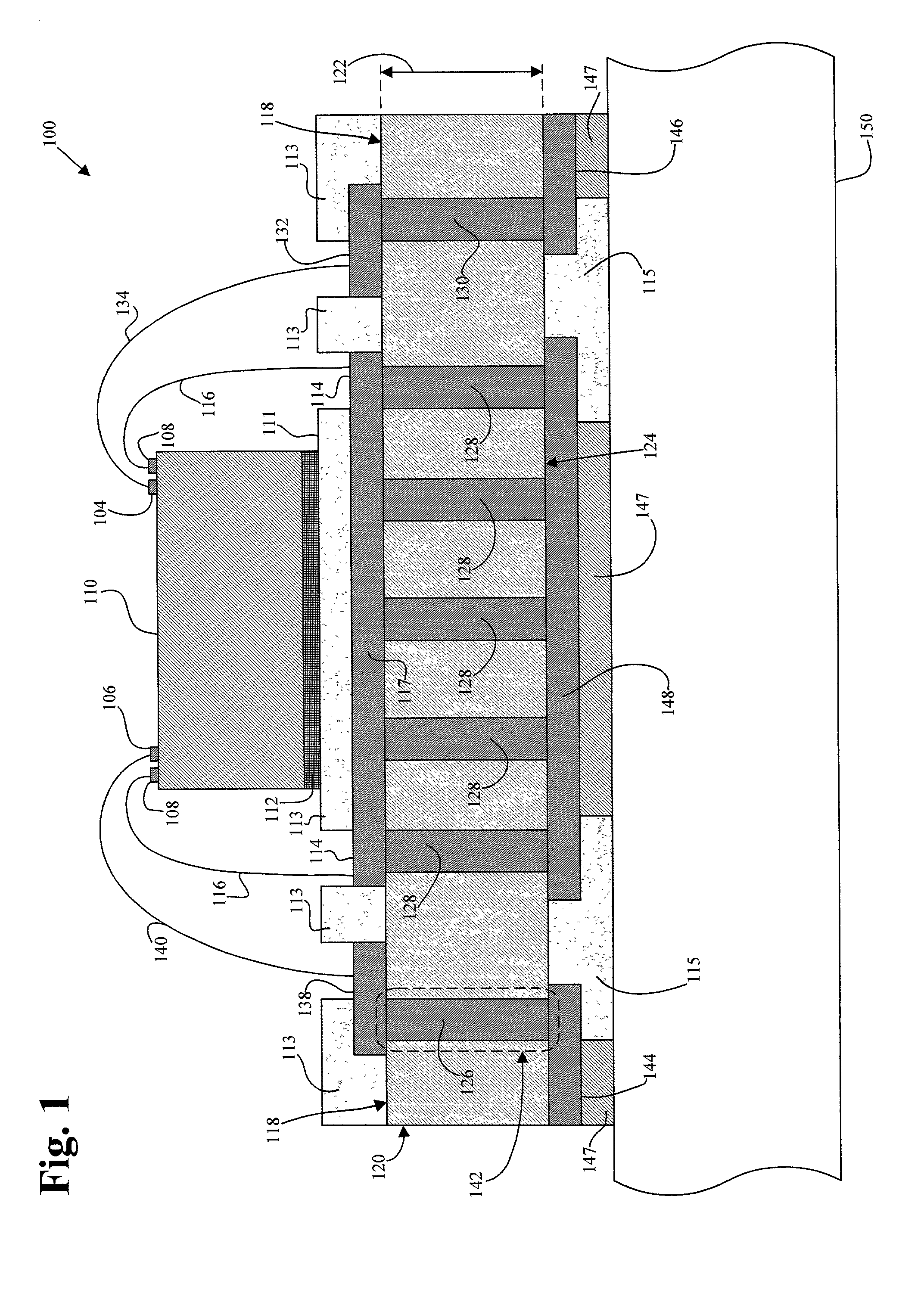
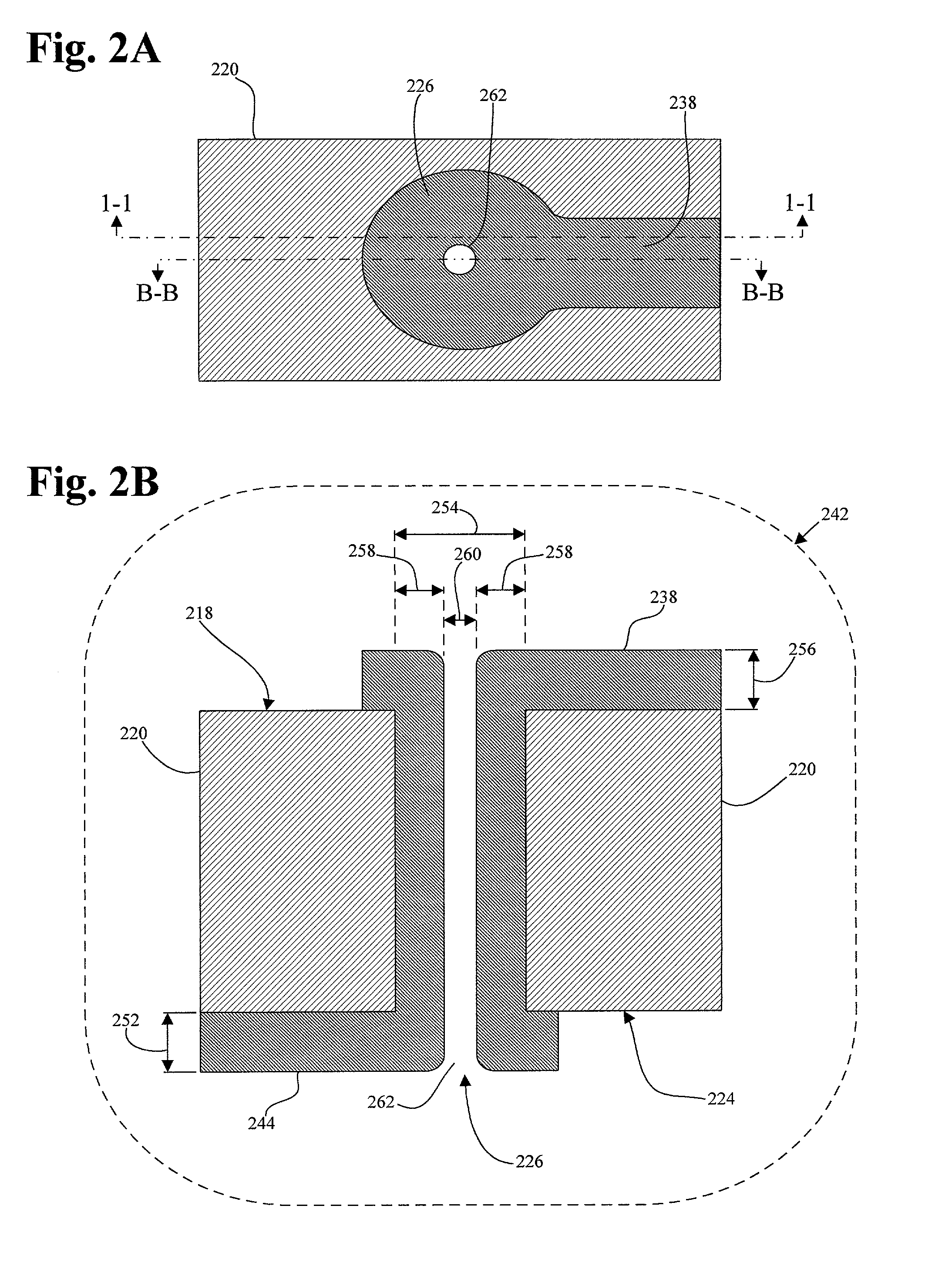
[0025]The present invention is directed structure and method for fabrication of a leadless chip carrier. The following description contains specific information pertaining to various embodiments and implementations of the invention. One skilled in the art will recognize that the present invention may be practiced in a manner different from that specifically discussed in the present application. Moreover, some of the specific details of the invention are not discussed in order not to obscure the invention. The specific details not described in the present application are within the knowledge of a person of ordinary skills in the art.

[0026]The drawings in the present application and their accompanying detailed description are directed to merely example embodiments of the invention. To maintain brevity, other embodiments of the invention that use the principles of the present invention are not specifically described in the present application and are not specifically illustrated by the...


PUM


Abstract

Structure and method for fabrication of a leadless chip carrier have been disclosed. A disclosed embodiment comprises a substrate having a top surface for receiving a semiconductor die. The disclosed embodiment also comprises a printed circuit board attached to a bottom surface of the substrate. The disclosed embodiment further comprises at least one via in the substrate, which provides an electrical connection between a signal bond pad of the semiconductor die and the printed circuit board. The at least one via also electrically connects a substrate bond pad and the printed circuit board. The substrate bond pad is further connected to the signal bond pad of the semiconductor die by a signal bonding wire. The at least one via further provides an electrical connection between the signal bond pad of the semiconductor die and a land that is electrically connected to the printed circuit board.

Description

[0001]This application is a continuation in part of, and claims benefit of the filing date of, and hereby incorporates fully be reference, the pending parent application entitled “Leadless Chip Carrier Design and Structure” Ser. No. 09 / 713,834 filed Nov. 15, 2000 and assigned to the assignee of the present application.BACKGROUND OF THE INVENTION[0002]1. Field of the Invention[0003]The present invention is generally in the field of semiconductor chip packaging. More specifically, the present invention is in the field of leadless chip carrier design and structure.[0004]2. Background Art[0005]The semiconductor fabrication industry is continually faced with a demand for smaller and more complex dies. These smaller and more complex semiconductor dies must also run at higher frequencies. The requirement of smaller, more complex, and faster devices has resulted in new challenges not only in the fabrication of the die itself but also in the manufacturing of various packages, structures, or ...

Claims


Application Information

Patent Timeline
Patent Type & Authority Patents(United States)
IPC IPC(8): H01L23/48H01L23/34H01L23/58H01L23/64H01L23/367H01L23/498H01L25/065
CPCH01L23/3677H01L23/49827H01L23/49838H01L23/64H01L23/645H01L24/49H01L25/0655H01L24/45H01L2223/6677H01L2224/16237H01L2224/45015H01L2224/45124H01L2224/45144H01L2224/48091H01L2224/48137H01L2224/48228H01L2224/48235H01L2224/48237H01L2224/49171H01L2924/01005H01L2924/01013H01L2924/01027H01L2924/01028H01L2924/01029H01L2924/01042H01L2924/01046H01L2924/01047H01L2924/01074H01L2924/01078H01L2924/01079H01L2924/01082H01L2924/09701H01L2924/14H01L2924/15313H01L2924/19042H01L2924/20753H01L2924/30105H01L2924/30107H01L2924/3025H01L2924/00014H01L24/48H01L2924/01033H01L2924/014H01L2224/48227H01L2224/73265H01L2224/32225H01L2924/00H01L2924/351H01L2924/15747H01L2924/15787H01L2924/181
Inventor HASHEMI, HASSAN S.COTE, KEVIN
Owner SKYWORKS SOLUTIONS INC
Why Eureka
Try Eureka