Single rank memory module for use in a two-rank memory module system

a memory module and single-rank technology, applied in the field of memory module configuration, can solve the problems of moving out of the sweet spot increasing the failure rate of the memory module,

Active Publication Date: 2005-11-01
ORACLE INT CORP
View PDF10 Cites 150 Cited by
  • Summary
  • Abstract
  • Description
  • Claims
  • Application Information

AI Technical Summary

Problems solved by technology

If the data path width increases due to an increase in the number of memory chips used to create the width, then the failure rate for the memory module increases.
Thus, if the number of components increases, then the failure rate for the memory module increases and the MTBF decreases.
Thus, if a purchaser continues to use older smaller capacity devices, the will move out of the sweet spot since the performance may no longer be in the desired range for a given cost model.
However in many cases, doing so may present system compatibility issues.

Method used


Image

  • Single rank memory module for use in a two-rank memory module system
  • Single rank memory module for use in a two-rank memory module system
  • Single rank memory module for use in a two-rank memory module system

Examples


Embodiment Construction

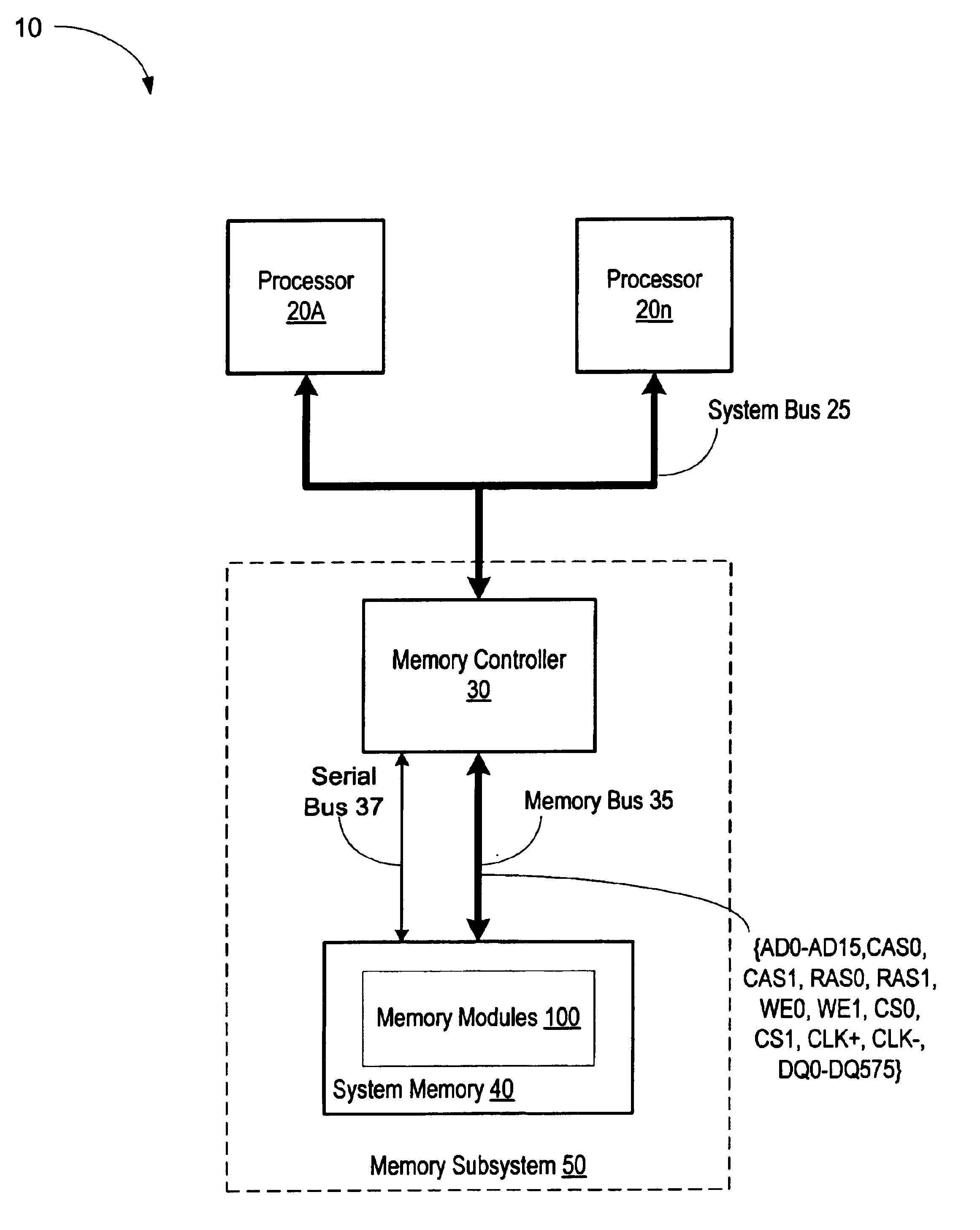
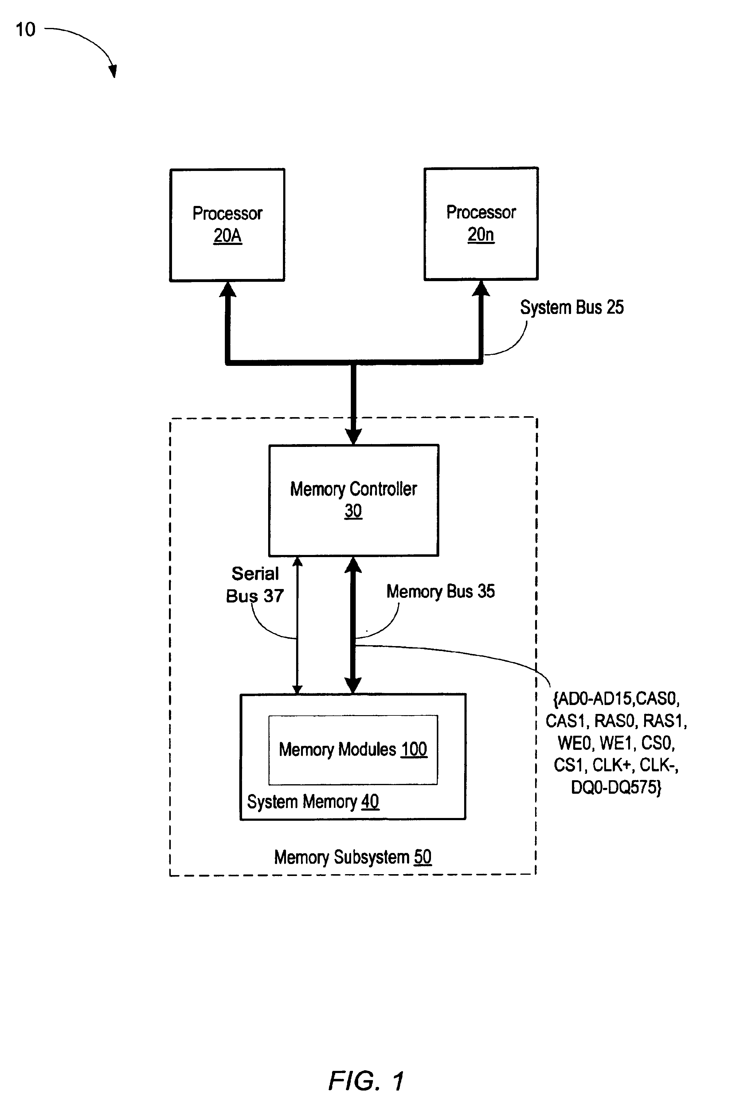
[0016]Turning now to FIG. 1, a block diagram of one embodiment of a computer system 10 is shown. Computer system 10 includes a plurality of processors 20-20n connected to a memory subsystem 50 via a system bus 25. Memory subsystem 50 includes a memory controller 30 coupled to a system memory 40 via a memory bus 35 and a serial bus 37. It is noted that, although two processors and one memory subsystem are shown in FIG. 1, embodiments of computer system 10 employing any number of processors and memory subsystems are contemplated. In addition, elements referred to herein with a particular reference number followed by a letter may be collectively referred to by the reference number alone. For example, processor 20A-n may be collectively referred to as processor 20.

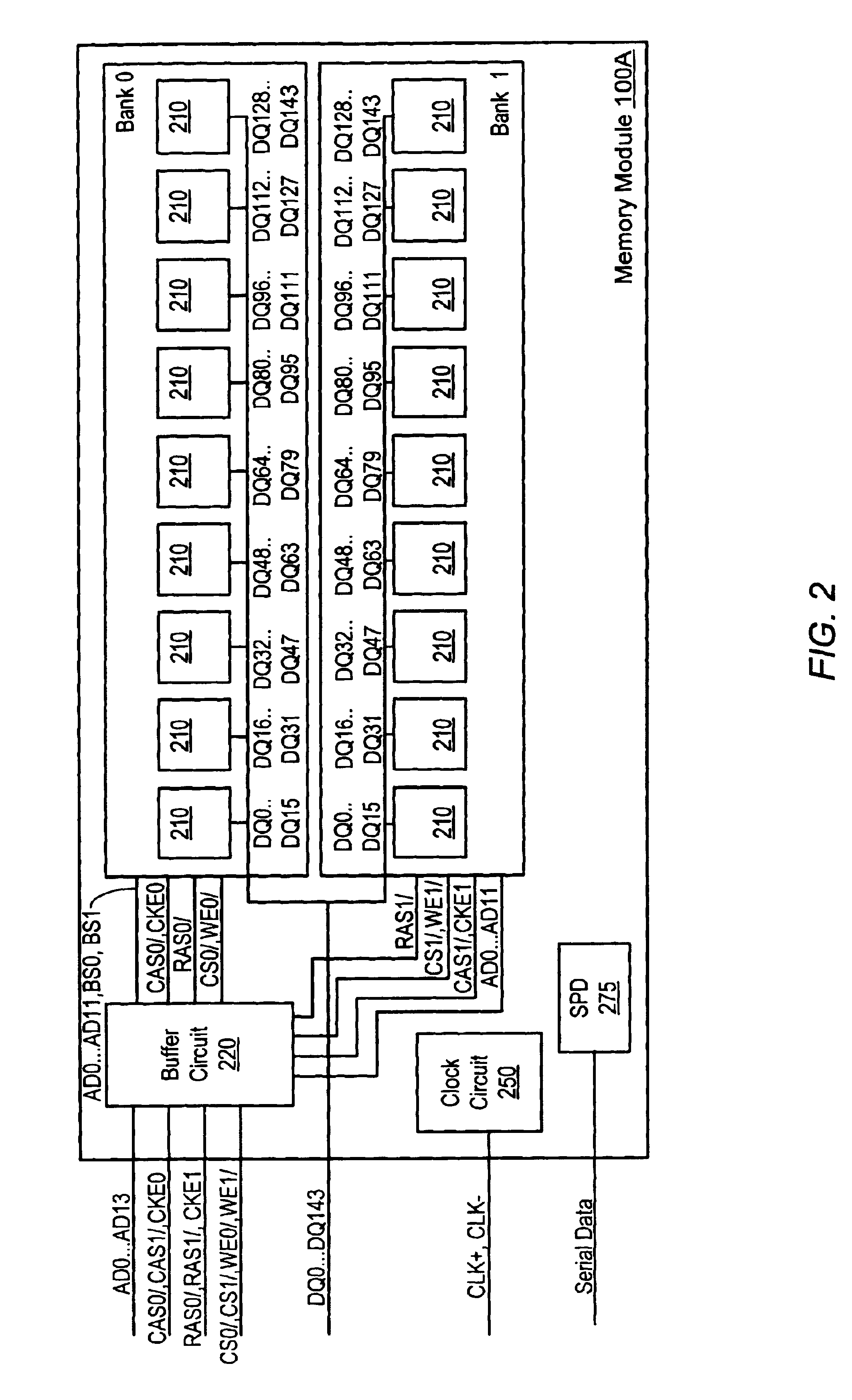
[0017]Memory subsystem 30 is configured to store data and instruction code within system memory 40 for use by processor 20. As will be described further below, in one embodiment, system memory 40 may be implemented using a plu...


PUM


Abstract

A memory module for use in a two rank memory module system includes a plurality of memory devices and a control circuit. In one embodiment, the control circuit may be configured to generate a chip select signal that is provided to each of the memory devices. The chip select signal may be dependent upon assertions of a first bank chip select signal and a second bank chip select signal received from a memory controller. The control circuit may be further configured to generate an address signal that is provided to each of the memory devices. The address signal may be asserted dependent upon which of the first bank chip select signal and the second bank chip select signal are asserted.

Description

BACKGROUND OF THE INVENTION[0001]1. Field of the Invention[0002]This invention relates to computer system memories and, more particularly, to memory module configurations.[0003]2. Description of the Related Art[0004]Many modern computer systems allow for memory expansion using memory modules. Two commonly used types of memory modules are single inline memory modules (SIMMs) and dual inline memory modules (DIMMs). SIMMs and DIMMs include small, compact circuit boards that are designed to mount easily into an expansion socket mounted on another circuit board, such as a computer system motherboard. The memory module circuit boards used to implement SIMMs and DIMMs include an edge connector that has contact pads or pins that are typically arranged on both sides of the circuit board. On SIMMs, opposing contact pads are connected together (i.e. shorted), and thus carry the same signal, while at least some of the opposing contact pads on DIMMs are not connected together, thus allowing diff...

Claims


Application Information

Patent Timeline
Patent Type & Authority Patents(United States)
IPC IPC(8): G06F12/06G11C5/02G11C5/04G11C8/00G11C8/12G06F13/42
CPCG06F12/0653G06F13/4243Y02B60/1235Y02B60/1228Y02B60/1225Y02D10/00G06F12/06G11C8/12
Inventor WONG, TAYUNGFANG, CLEMENT C.JEFFREY, DAVID J.DUNCAN, NEIL N.
Owner ORACLE INT CORP
Why Eureka
Try Eureka