Method of manufacturing a semiconductor device having leads stabilized during die mounting

Inactive Publication Date: 2005-11-08
RENESAS ELECTRONICS CORP
View PDF17 Cites 0 Cited by
  • Summary
  • Abstract
  • Description
  • Claims
  • Application Information

AI Technical Summary

Benefits of technology

[0030]According to the present invention, since thickness of the insulating member can be made thin, the thermal conduction can be improved at the time of die bonding.
[0031]In addition, since th

Problems solved by technology

However, techniques described in the above-mentioned seven Japanese Patent Laid-Open references except for Japanese Patent Laid-Open No. 5-235246 have objects of improving heat radiation properties thereof by using metal sheets or ceramic sheets, and do not disclose the concept that a technique for fixing inner leads to metal sheets or ceramic sheets via adhesives is used for semiconductor devices having many pins and narrow pad pitches.
But, in the construction (the construction in which the main surface of the semiconductor chip is fixed to one surface of the insulation tape, and the inner lead is fixed in the other surface t

Method used


Image

  • Method of manufacturing a semiconductor device having leads stabilized during die mounting
  • Method of manufacturing a semiconductor device having leads stabilized during die mounting
  • Method of manufacturing a semiconductor device having leads stabilized during die mounting

Examples


Example

(Embodiment 1)

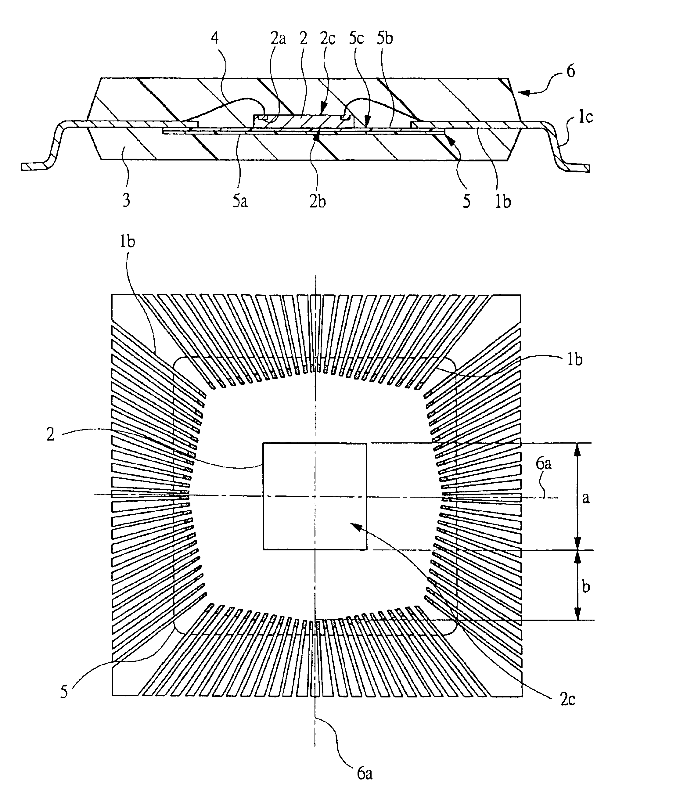
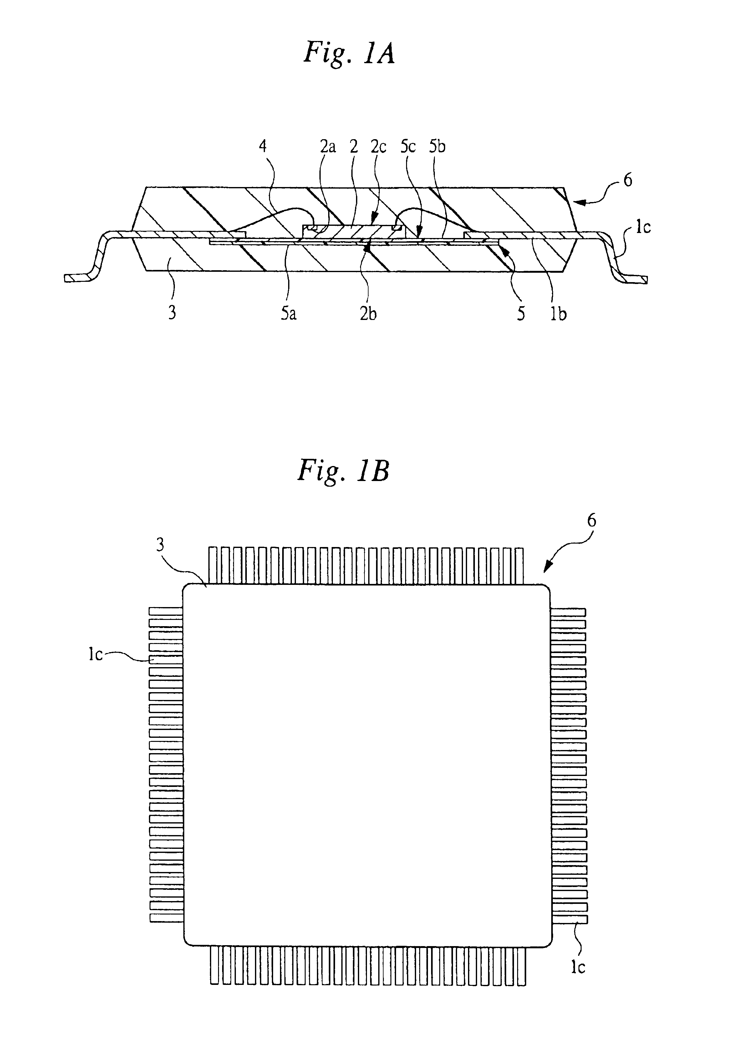
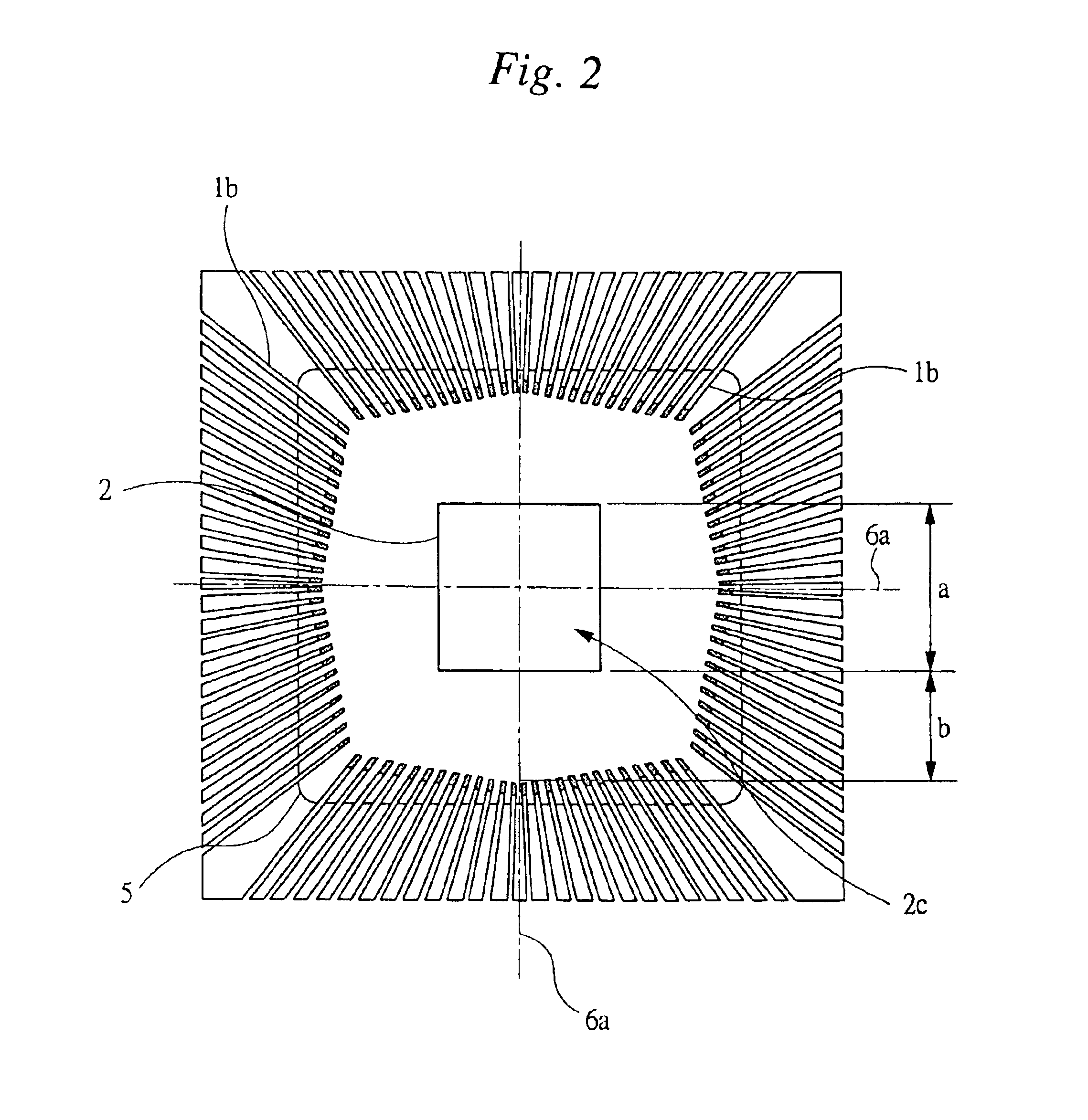
[0078]FIGS. 1A and 1B are views showing one example of a construction of a semiconductor device that is Embodiment 1 of the present invention, wherein FIG. 1A shows a cross-sectional view and FIG. 1B shows a plan view. FIG. 2 is a partial plan view showing one example of a distance between a semiconductor chip and respective inner leads in the semiconductor device shown in FIG. 1. FIG. 3 is a partial enlarged plan view showing one example of a pad pitch between adjacent semiconductor chips and of a lead pitch between adjacent inner leads in the semiconductor device shown in FIG. 1. FIG. 4 is a partial plan view shown by partially cutting away one example of a construction of the matrix frame used for assembly of the semiconductor device shown in FIG. 1. FIG. 5 is a partially enlarged cross-sectional view showing a structure having a cross section taken along line A—A in FIG. 4. FIG. 6 is a partial plan view shown by partially cut away one example of a construction form...

Example

(Embodiment 2)

[0139]FIG. 26 is a cross-sectional view showing one example of a construction of a semiconductor device that is Embodiment 2 of the present invention. FIG. 27 is a partial cross-sectional view showing one example of a construction of a lead frame used for assembly of the semiconductor device shown in FIG. 26. FIGS. 28 to 33 are partial cross-sectional views showing constructions of lead frames of modified examples that are Embodiment 2 of the present invention. FIG. 34 is a partial cross-sectional view showing one example of thickness relationships between a semiconductor chip, an insulating member, and an adhesive layer when the semiconductor chip is mounted to the insulating member of the lead frame that is Embodiment 2 of the present invention. FIG. 35 and FIG. 36 are partially enlarged plan views showing constructions of lead frames of modified examples that are Embodiment 2 of the present invention.

[0140]The semiconductor device of Embodiment 2 shown in FIG. 26 is...


PUM


Abstract

A semiconductor device comprises a plurality of inner leads extending around a semiconductor chip, a tape substrate supporting the semiconductor chip and joined to respective end portions of the inner leads, wires connecting the inner leads and pads formed on a main surface of the semiconductor chip, a seal portion formed by resin-sealing the semiconductor chip and the wires, and a plurality of outer leads linking in a line with the inner leads and protruded from the seal portion to the exterior of four directions. A relationship between a length (a) of a shorter side of the semiconductor chip and a clearance (b) from the semiconductor chip, to a tip of the inner leads arranged at the farthest location from the semiconductor chip is a≦2b. It is possible to attain a narrow pad pitch, and mount the semiconductor chip formed in a small size, and standardize the lead frame.

Description

[0001]This is a divisional application of U.S. Ser. No. 09 / 978,708, filed Oct. 18, 2001, now U.S. Pat. No. 6,661,081.BACKGROUND OF THE INVENTION[0002]The present invention relates to a semiconductor manufacturing technique, and in particular, to an effective technique applied to enhancement of the reliability of semiconductor devices having small semiconductor chips arranged at narrow pad pitches.[0003]In Japanese Patent Laid-Open No. 8-116012, No. 5-160304, No. 5-36862, No. 11-289040, No. 11-514149, No. 7-153890, No. 6-291217 and No. 5-235246, there are disclosed techniques for fixing inner leads to metal sheets and ceramic sheets via adhesives or the like.[0004]Firstly, in Japanese Patent Laid-Open No. 8-116012, there is disclosed a resin-sealing type semiconductor device in which an aluminum sheet is used as a heat radiation plate and the inner lead is fixed to the aluminum sheet via adhesives by providing an insulation layer on a surface of the aluminum sheet. There are describe...

Claims


Application Information

Patent Timeline
IPC IPC(8): H01L23/48H01L23/495H01L23/50
CPCH01L23/49506H01L2224/48091H01L2224/48247H01L2224/49171H01L2924/01039H01L2924/01057H01L2224/45144H01L2924/09701H01L2924/14H01L2924/01079H01L2924/07802H01L24/48H01L24/49H01L2924/00014H01L2924/00H01L24/45H01L2924/181H01L2224/73265H01L2224/05599H01L2924/00012H01L23/50
Inventor MIYAKI, YOSHINORISUZUKI, HIROMICHI
Owner RENESAS ELECTRONICS CORP
Why Eureka
Try Eureka