

Underfill film, sealing sheet, method of manufacturing semiconductor device, and semiconductor device
- Summary
- Abstract
- Description
- Claims
- Application Information
AI Technical Summary
Benefits of technology
Problems solved by technology
Method used
Image

Examples
embodiment 1
[0108]The method of manufacturing a semiconductor device of Embodiment 1 is explained. FIGS. 2A to 2I are views showing each step of the method of manufacturing a semiconductor device of Embodiment 1.
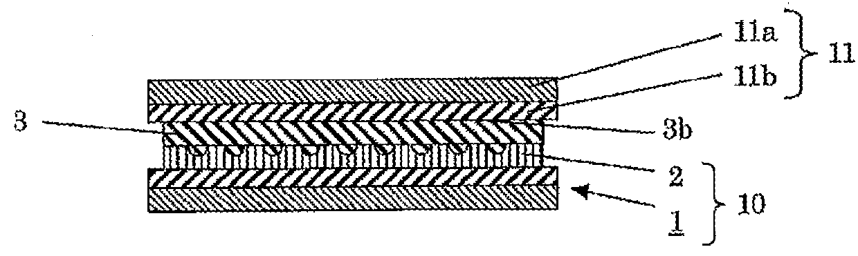
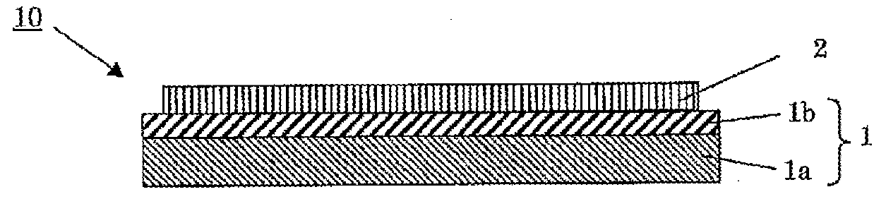
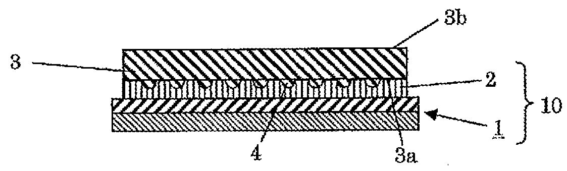
[0109]The sealing sheet 10 is used in Embodiment 1.
[0110]The method of manufacturing a semiconductor device of Embodiment 1 includes a bonding step of bonding a circuit surface 3a on which a connection members 4 of the semiconductor wafer 3 are formed and the underfill film 2 of the sealing sheet 10 together, a grinding step of grinding a rear surface 3b of the semiconductor wafer 3, a wafer fixing step of bonding a dicing tape 11 to the rear surface 3b of the semiconductor wafer 3, a peeling step of peeling the pressure-sensitive adhesive tape 1, a dicing position determination step of irradiating the exposed surface of the underfill film 2 of the semiconductor wafer 3 with the underfill film 2 with oblique light L to determine a dicing position, a dicing step of dicing the semiconduct...
embodiment 2
[0156]The method of manufacturing a semiconductor device of Embodiment 2 is explained. FIGS. 5A to 5E are views showing each step of the method of manufacturing a semiconductor device of Embodiment 2.
[0157]The sealing sheet 10 is used in Embodiment 2.
[0158]The method of manufacturing a semiconductor device of Embodiment 2 includes a bonding step of bonding a semiconductor wafer 43 on which a circuit surface having connection members 44 is formed on both surfaces and the underfill film 2 of the sealing sheet 10 together, a dicing step of dicing the semiconductor wafer 43 to form a semiconductor chip 45 with the underfill film 2, a pickup step of peeling the semiconductor chip 45 with the underfill film 2 from the pressure-sensitive adhesive tape 1, a position matching step of irradiating the exposed surface of the underfill film 2 of the semiconductor element 45 with the underfill film 2 with the oblique light L to match the relative positions of the semiconductor element 45 and the ...
embodiment 3
[0172]The method of manufacturing a semiconductor device of Embodiment 3 is explained. Embodiment 3 is the same one as Embodiment 1 except that the underfill film is provided on the base. The same base as the base 1a can be used as the base.
PUM
| Property | Measurement | Unit |
|---|---|---|
| Fraction | aaaaa | aaaaa |
| Fraction | aaaaa | aaaaa |
| Fraction | aaaaa | aaaaa |
Abstract
Description
Claims
Application Information