Devices incorporating electrochromic elements and optical sensors

a technology of optical sensors and electrochromic elements, which is applied in the direction of optical radiation measurement, printers, lenses, etc., can solve the problems of sensor washout at a high light level, excessively long scan time for dim scenes, and high cost of packaging assemblies

Inactive Publication Date: 2005-11-08
GENTEX CORP
View PDF18 Cites 50 Cited by
  • Summary
  • Abstract
  • Description
  • Claims
  • Application Information

AI Technical Summary

Benefits of technology

[0024]In a further embodiment, the optical sensor is coated with a transparent curable resin to provide environmental protection.

Problems solved by technology

These packaging assemblies are expensive and difficult to manufacture.
As an example, a configuration allowing the sensor to operate at low light levels may cause the sensor to wash out at a high light level.
Since the scan time is generally a multiple of the integration time, a camera set to 30 milliseconds scan period for a bright scene may result in an excessively long scan time for a dim scene.
Further, particularly if a lens is used to focus light on the sensor, direct exposure to sunlight can generate sufficient heat to damage sensor elements.
Electrically attenuated grayscale filters are never part of the commercial sensor device package, if available at all.

Method used


Image

  • Devices incorporating electrochromic elements and optical sensors
  • Devices incorporating electrochromic elements and optical sensors
  • Devices incorporating electrochromic elements and optical sensors

Examples


Embodiment Construction

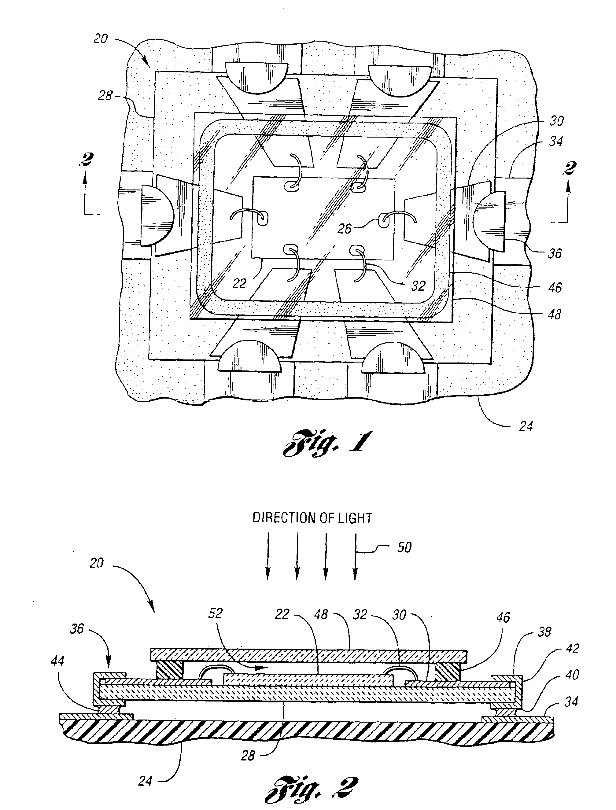
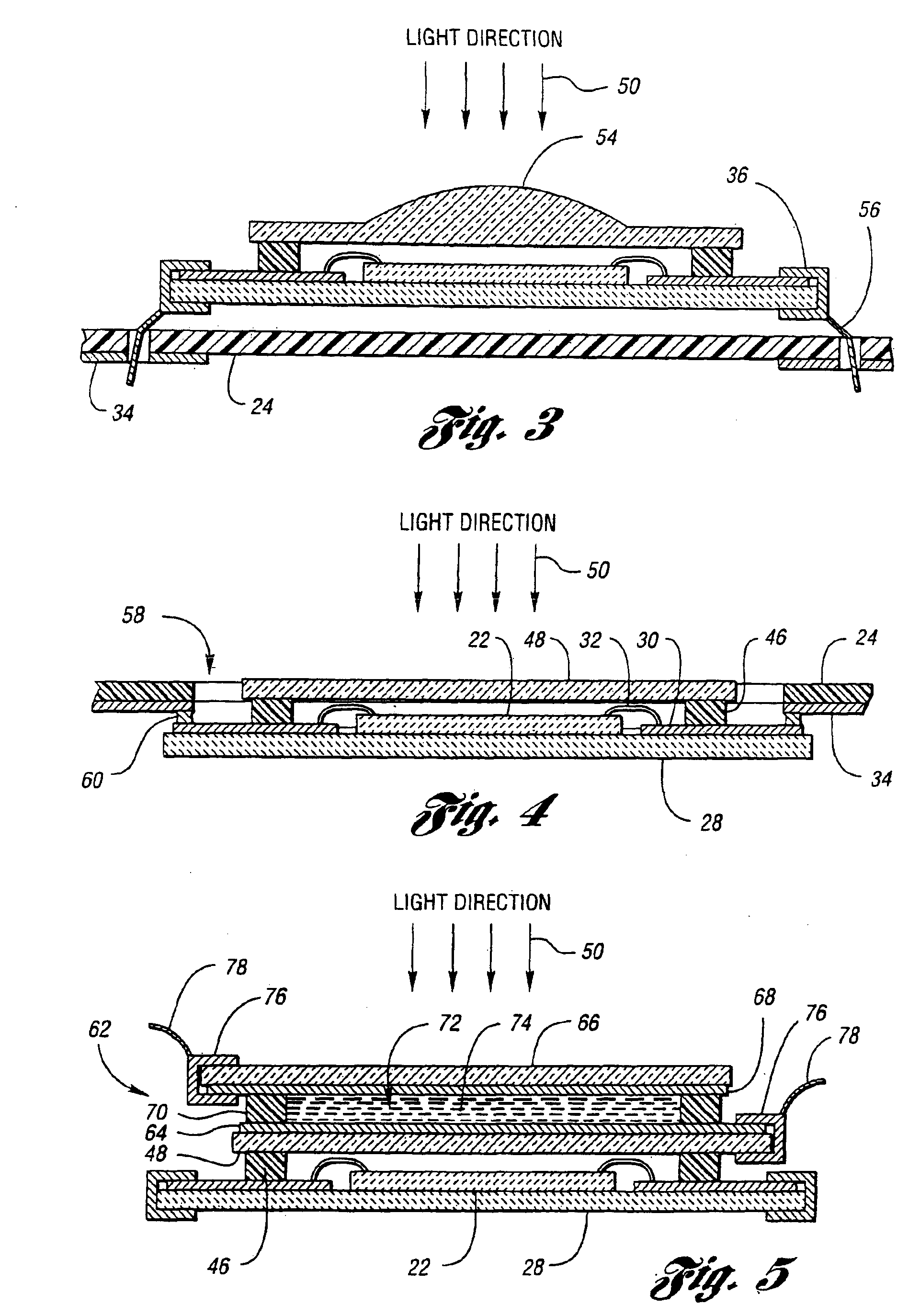
[0046]Referring now to FIGS. 1 through 5 and 8 through 17, drawings of embodiments of the present invention are shown. These drawings are not to scale and are provided to show the relationships amongst various elements used to construct the optical sensor package. Further, directional designations such as top and bottom are used for clarity of explanation and are not meant to restrict the present invention to any particular orientation.

[0047]Referring now to FIG. 1, an overhead view, and to FIG. 2, a cross-sectional view, an embodiment of the present invention is shown. An enclosure assembly 20 is provided to encapsulate an optical sensor 22. Enclosure assembly 20 is designed to be mounted on a support substrate 24 which may be, for example, a printed circuit board, flexible circuit, ceramic substrate, or the like.

[0048]Optical sensor 22 is an integrated circuit chip. Optical sensor 22 may be, for example, an image sensor including an array of pixel sensors and support electronics. ...


PUM

PropertyMeasurementUnit
scan timeaaaaaaaaaa
thicknessaaaaaaaaaa
thicknessaaaaaaaaaa

Abstract

The device of the present invention includes an electrochromic element having a transmittance that varies in response to an electrical signal, a base substrate disposed in spaced relation to the electrochromic element, a seal disposed between the base substrate and the electrochromic element, and an optical sensor. The seal, base substrate, and electrochromic element form a sealed cavity therebetween, in which the optical sensor is disposed. According to another embodiment, an electrochromic device is provided that includes a first substrate, an electrochromic medium disposed on the first substrate, a pair of electrodes in contact with the electrochromic medium, a pair of conductive clips, each in electrical contact with a respective one of the electrodes, and two pairs of electrical lead posts for mounting the first substrate to the circuit board. Each pair of lead posts is attached to, and extends from, a respective one of the conductive clips. According to another embodiment, an imaging device is disclosed having an image recorder for recording a scene or object, and an electrochromic element positioned between the image recorder and the object or scene to be imaged. The electrochromic element is configured to exhibit a non-uniform transmittance in response to an applied electrical signal.

Description

[0001]This application is a continuation of U.S. patent application Ser. No. 09 / 678,586 filed on Oct. 3, 2000, now U.S. Pat. No. 6,621,616, by Frederick T. Bauer et al. which is entitled “DEVICES INCORPORATING ELECTROCHROMIC ELEMENTS AND OPTICAL SENSORS”. The present invention generally relates to electrochromic devices and devices incorporating electrochromic elements, such as devices incorporating both electrochromic elements and optical sensors, the disclosure of which is incorporated herein by reference.BACKGROUND OF THE INVENTION[0002]Variable transmittance light filters, such as electrochromic light filters, have been proposed for many uses including in architectural windows; skylights; rearview mirrors, windows, and sunroofs for automobiles; and in certain imaging systems. Such electrochromic light filters respond to a change in applied voltage by changing their transmittance. In general, it has been a goal of designers of electrochromic elements to configure the elements to ...

Claims


Application Information

Patent Timeline
Patent Type & Authority Patents(United States)
IPC IPC(8): H04N5/225G02F1/01G02F1/153H01L27/146H01L31/0203H01L31/0232
CPCH01L27/14618H01L27/14625H01L31/0203H01L31/0232H04N5/2253H04N5/2254G02F1/153H01L2224/48091H01L2924/00014H01L2224/48227G02F2203/48G03B9/02H01L31/02325H04N23/54H04N23/55
Inventor BAUER, FREDERICK T.STAM, JOSEPH S.
Owner GENTEX CORP
Why Eureka
Try Eureka