White light-emitting OLED device having a blue light-emitting layer doped with an electron-transporting or a hole-transporting material or both

a light-emitting oled, blue light-emitting layer technology, applied in the direction of discharge tube luminescnet screen, other domestic articles, natural mineral layered products, etc., can solve the problems of difficult control of large-scale manufacturing process, color filter transmits only about 30% of original light, and achieves improved device efficiency and operational stability, high reproducibility and consistency, and high efficiency

Inactive Publication Date: 2005-11-22
GLOBAL OLED TECH
View PDF5 Cites 60 Cited by
  • Summary
  • Abstract
  • Description
  • Claims
  • Application Information

AI Technical Summary

Problems solved by technology

These concentrations are difficult to control during large-scale manufacturing.
However, these OLED devices require very small amounts of dopant concentrations, making the process difficult to control for large-scale manufacturing.
However, the color filter transmits only about 30% of the original light.
This reduces the lifetime of the blue color.

Method used


Image

  • White light-emitting OLED device having a blue light-emitting layer doped with an electron-transporting or a hole-transporting material or both
  • White light-emitting OLED device having a blue light-emitting layer doped with an electron-transporting or a hole-transporting material or both
  • White light-emitting OLED device having a blue light-emitting layer doped with an electron-transporting or a hole-transporting material or both

Examples


Embodiment Construction

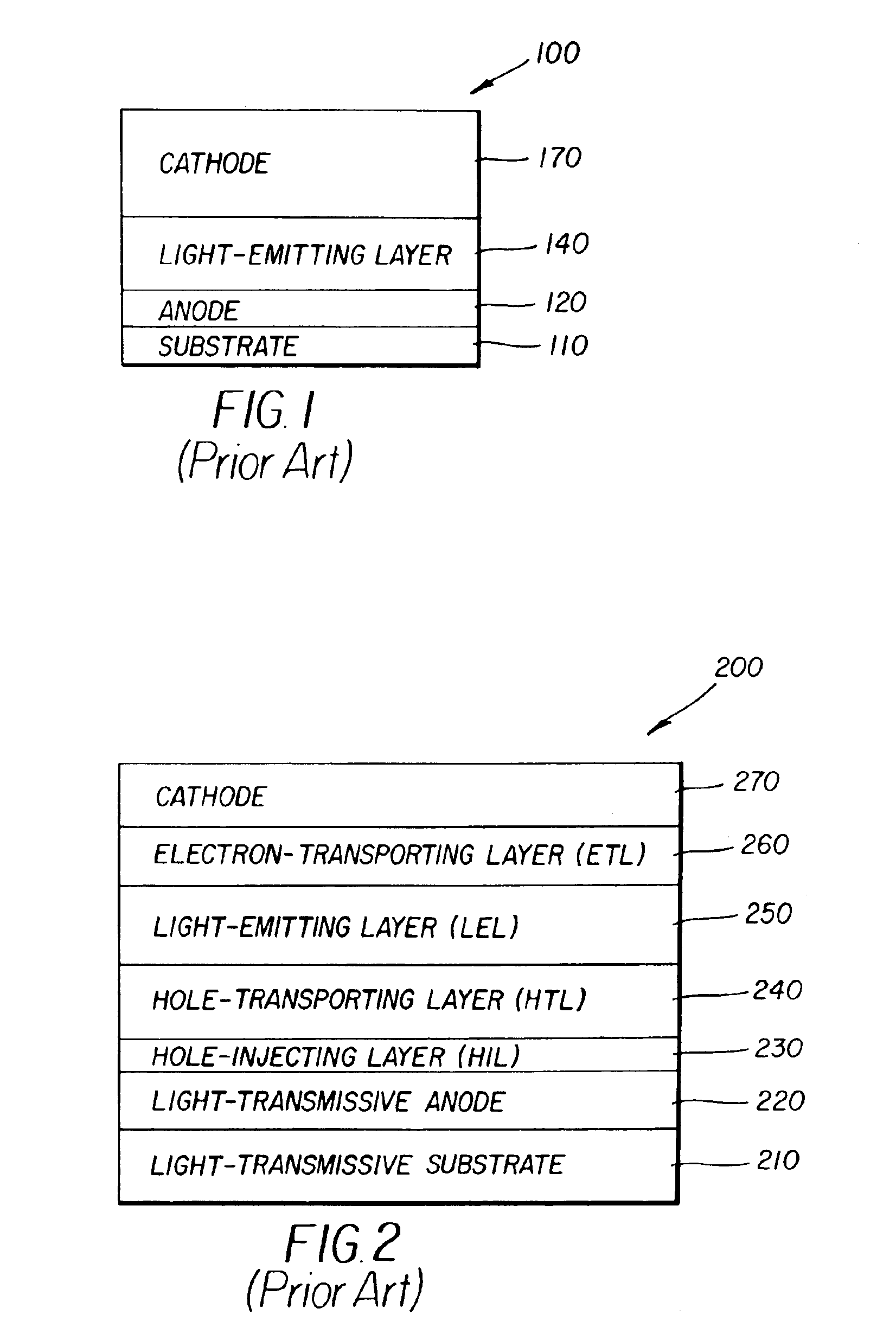
[0035]A conventional light-emitting layer of the organic OLED device comprises a luminescent or fluorescent material where electroluminescence is produced as a result of electron-hole pair recombination in this region. In the simplest construction, the device 100 as shown in FIG. 1 has a substrate 110 and a light-emitting layer 140 sandwiched between anode 120 and cathode 170. The light-emitting layer 140 is a pure material with a high luminescent efficiency. A well known material is tris(8-quinolinato) aluminum (Alq) which produces excellent green electroluminescence.

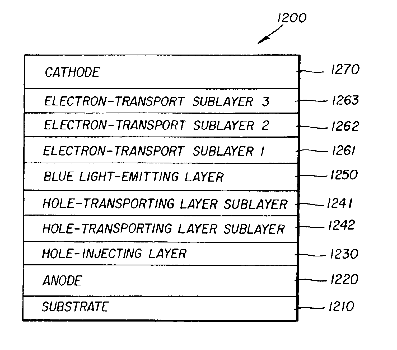
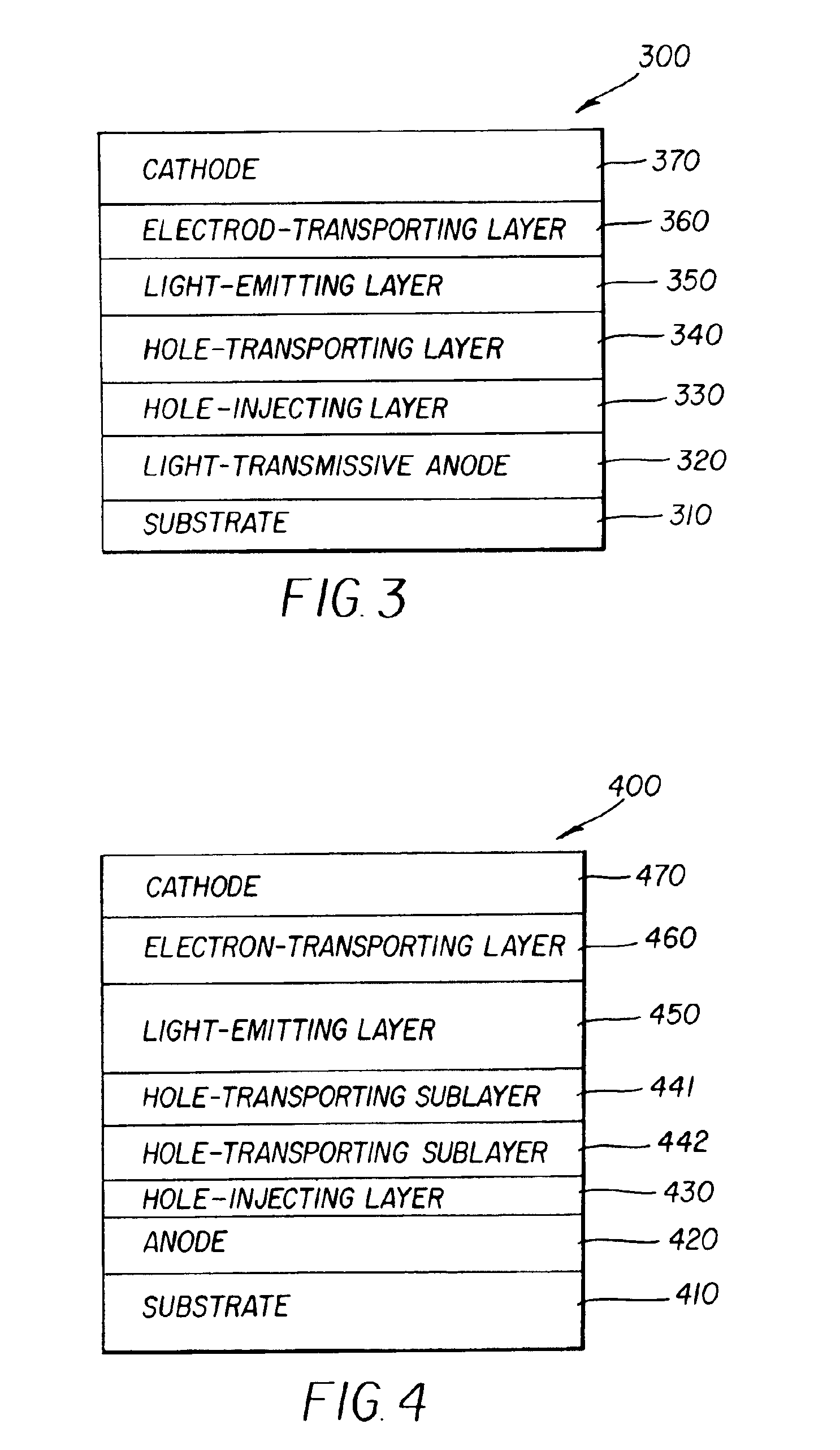
[0036]The simple structure can be modified to a three-layer structure (device 200) as shown in FIG. 2, in which an additional electroluminescent layer is introduced between the hole- and electron-transporting layers to function primarily as the site for hole-electron recombination and thus electroluminescence. In this respect, the functions of the individual organic layers are distinct and can therefore be optimized in...


PUM

PropertyMeasurementUnit
work functionaaaaaaaaaa
wavelengthsaaaaaaaaaa
current densityaaaaaaaaaa

Abstract

An organic light-emitting diode (OLED) device which produces substantially white light includes an anode; a hole-transporting layer disposed over the anode; and a blue light-emitting layer having a host doped with a blue light-emitting compound disposed directly on the hole-transporting layer and the blue light-emitting layer being doped with an electron-transporting or a hole-transporting material or both selected to improve efficiency and operational stability. The device also includes an electron-transporting layer disposed over the blue light-emitting layer; a cathode disposed over the electron-transporting layer; and the hole-transporting layer or electron-transporting layer, or both the hole-transporting layer and electron-transporting layer, being selectively doped with a compound which emits light in the yellow region of the spectrum which corresponds to an entire layer or a partial portion of a layer in contact with the blue light-emitting layer.

Description

CROSS REFERENCE TO RELATED APPLICATIONS[0001]This is a continuation-in-part of application Ser. No. 10 / 391,727, filed Mar. 19, 2003 now abandoned entitled “White Light-Emitting OLED Device Having a Blue Light-Emitting Layer Doped With an Electron-Transporting or a Hole-Transporting Material or Both” by Tukaram K. Hatwar et al.[0002]Reference is made to commonly assigned U.S. patent application Ser. No. 09 / 651,624 filed Aug. 30, 2000, now U.S. Pat. No. 6,699,177 issued Feb. 24, 2004, by Tukaram K. Hatwar, entitled “White Organic Electroluminescent Devices with Improved Stability and Efficiency”; Ser. No. 10 / 191,251 filed Jul. 8, 2002, now U.S. Pat. No. 6,720,092 issued Apr. 13, 2004, by Tukaram K. Hatwar, entitled “White Organic Light-Emitting Devices Using Rubrene Layer”; Ser. No. 10 / 183,242 filed Jun. 27, 2002, now U.S. Pat. No. 6,661,013 issued Dec. 19, 2003, by Benjamin P. Hoag et al., entitled “Organic Element for Electroluminescent Devices”; Ser. No. 10 / 086,067 filed Feb. 28, 2...

Claims


Application Information

Patent Timeline
Patent Type & Authority Patents(United States)
IPC IPC(8): H05B33/14H01L51/50C09K11/06H01L27/00H01L33/00H01L51/00H01L51/30H05B33/00H05B33/22
CPCH01L51/5036C09K11/06H01L51/5064C09K2211/107H01L51/0052H01L51/0059H01L51/0062H01L51/008H01L51/0081Y02B20/181C09K2211/1011C09K2211/1029Y10S428/917Y02B20/00H10K85/649H10K85/615H10K85/631H10K85/322H10K85/324H10K50/13H10K50/156H10K50/125
Inventor HATWAR, TUKARAM K.RICKS, MICHELE L.WINTERS, DUSTINSPINDLER, JEFFREY P.
Owner GLOBAL OLED TECH
Why Eureka
Try Eureka