Organic electroluminescent device

a technology of electroluminescent devices and organic materials, applied in the direction of organic semiconductor devices, thermoelectric devices, solid-state devices, etc., can solve problems such as efficiency improvement, and achieve the effects of reducing the luminous efficiency of green emitting layers, preventing luminous efficiency reduction, and improving mass productivity

Inactive Publication Date: 2010-12-16
IDEMITSU KOSAN CO LTD
View PDF9 Cites 62 Cited by
  • Summary
  • Abstract
  • Description
  • Claims
  • Application Information

AI Technical Summary

Benefits of technology

[0076]In the green emitting layer 34 of the organic EL device of the invention, the difference between the affinity of the host GH and the affinity of the material constituting the electron-transporting layer is 0.4 eV or less.
[0077]Normally, the triplet energy of the phosphorescent dopant PGD of the green emitting layer is larger than the triplet energy ETel of the material constituting the electron-transporting layer. Therefore, prior to phosphorescent emission, the triplet excitons on the phosphorescent dopant PGD transfer to the material constituting the electron-transporting layer of which the triplet energy is smaller. As a result, luminous efficiency of the green emitting layer is lowered. However, as in the case of the invention, when the difference between the affinity of the host GH and the affinity of the material constituting the electron-transporting layer is allowed to be 0.4 eV or less, the injection properties of electrons from the electron-transporting layer to the green emitting layer is improved. As a result, electrons and holes are recombined in the hole-transporting region side of the emitting layer in a biased manner, that is, electrons and holes are recombined at a distance from the electron-transporting region. As a result, triplet excitons are generated at a distance from the green emitting layer, triplet excitons hardly transfer from the green emitting layer to the electron-transporting layer, whereby lowering in luminous efficiency can be prevented.
[0078]In addition, in order to keep the recombination region away from the electron-transporting layer, the hole mobility μh and the electron mobility μe of the host of the emitting layer desirably satisfies the relationship μe / μh>1. μe / μh>5 is most desirable.
[0079]As mentioned above, in the invention, emitting layers of three colors are formed in parallel. However, mass productivity is improved since a common material is used as the electron-transporting layer. Further, in the blue emitting layer, the luminous efficiency thereof is improved by utilizing the TTF phenomenon. In the green emitting layer, the luminous efficiency thereof is prevented from lowering by adjusting the affinity. As a result, a high efficiency is attained in both the blue emitting layer and the green emitting layer.
[0080]The red emitting layer 36 can be formed such that it contains a host RH and a phosphorescent dopant PRD. If the red emitting layer 36 contains the host RH and the phosphorescent dopant PRD, it is preferred that the difference between the affinity of the host RH and the affinity of the material constituting the electron-transporting layer is 0.4 eV or less. The reason therefor is that, as mentioned above, luminous efficiency is prevented from lowering since the transfer of triplet energy from the red emitting layer to the electron-transporting layer becomes difficult.
[0081]Also, it is preferred that the difference between the affinity of the host BH of the blue emitting layer and the affinity of the material constituting the electron-transporting layer be 0.4 eV or less. The reason therefor is that electron injecting properties to the emitting layer are improved by allowing the difference in affinity to be 0.4 eV or less. When the electron injecting properties to the emitting layer are deteriorated, the density of triplet excitons is decreased since the electron-hole recombination in the emitting layer is decreased. If the density of triplet excitons is decreased, the frequency of collision of triplet excitons is reduced, and a TTF phenomenon does not occur efficiently. Further, since electron injection performance is improved, the organic EL device can be driven at a lower voltage.

Problems solved by technology

In a phosphorescent device, efficient confinement of triplet excitons within an emitting layer does not necessarily result in improvement in efficiency.

Method used


Image

  • Organic electroluminescent device
  • Organic electroluminescent device
  • Organic electroluminescent device

Examples


example 1

[0166]The following materials for forming layers were sequentially deposited on a substrate on which a 130 nm thick ITO film to obtain an organic EL device.

[0167]Anode: ITO (film thickness; 130 nm)

[0168]Hole-injecting layer: HI (film thickness; 50 nm)

[0169]Hole-transporting layer: HT (film thickness; 45 nm)

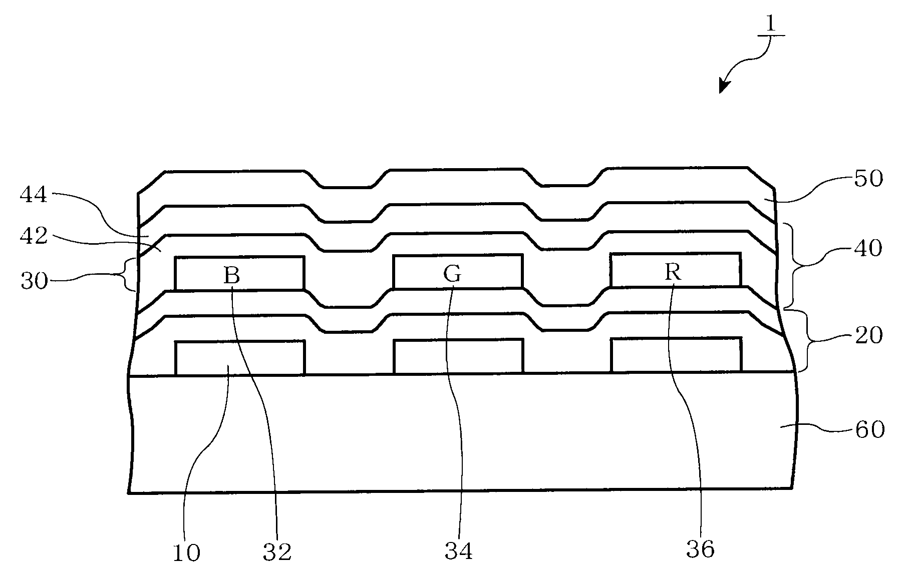
[0170]Emitting layer: (film thickness; blue 25 nm, green 50 nm, red 40 nm)[0171]Blue emitting layer BH—1: BD—1 (5 wt %)[0172]Green emitting layer GH—1: Ir(Ph-ppy)3 (10 wt %)[0173]Red emitting layer RH—1: Ir(piq)3 (10 wt %)

[0174]Electron-transporting layer (ETL): ET1 (film thickness; 5 nm)

[0175]LiF: (film thickness 1 nm)

[0176]Cathode: Al (film thickness: 80 nm)

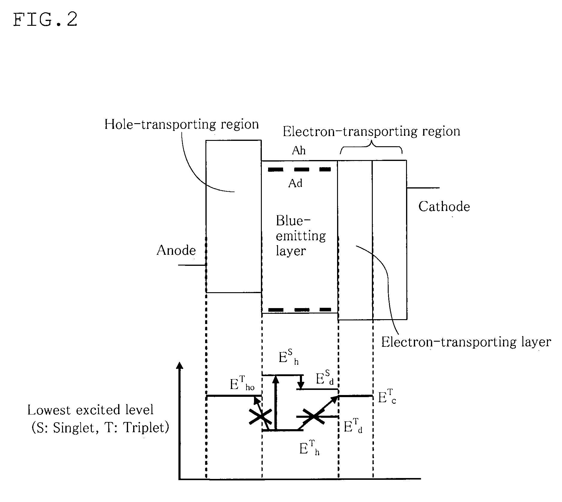
[0177]The blue emitting layer, green emitting layer and red emitting layer of the device obtained were caused to emit light by applying a DC of 1 mA / cm2 and the luminous efficiency thereof was measured (unit: cd / A). A continuous current test of DC was conducted at the following initial luminance to measure the half life (unit...

example 6

[0182]The following materials for forming layers were sequentially deposited on a substrate on which a 130 nm thick ITO film to obtain an organic EL device.

[0183]The organic EL device obtained was evaluated in the same manner as in Example 1. The results are shown in Table 1.

[0184]Anode: ITO (film thickness; 130 nm)

[0185]Hole-injecting layer: HI (film thickness; 50 nm)

[0186]Hole-transporting layer: HT (film thickness; 45 nm)

[0187]Emitting layer: (film thickness; blue 25 nm, green 50 nm, red 40 nm)[0188]Blue emitting layer BH—2: BD—2 (5 wt %)[0189]Green emitting layer GH—1: Ir(Ph-ppy)3 (10 wt %)[0190]Red emitting layer RH—1: Ir(piq)3 (10 wt %)

[0191]Electron-transporting layer (ETL): ET2 (film thickness; 5 nm)

[0192]Electron-injecting layer (EIL): EI1 (film thickness; 20 nm)

[0193]LiF: (film thickness 1 nm)

[0194]Cathode: Al (film thickness: 80 nm)


PUM


Abstract

An organic electroluminescence device including opposite anode and cathode, and a hole-transporting region, an emitting layer and an electron-transporting region in sequential order from the anode between the anode and the cathode, wherein the emitting layer is formed of a red emitting layer, a green emitting layer, and blue emitting layer; the blue emitting layer contains a host BH and a fluorescent dopant FBD; the triplet energy ETfbd of the fluorescent dopant FBD is larger than the triplet energy ETbh of the host BH; the green emitting layer contains a host GH and a phosphorescent dopant PGD; a common electron-transporting layer is provided adjacent to the red emitting layer, the green emitting layer and the blue emitting layer within the electron-transporting region; the triplet energy ETel of a material constituting the electron-transporting layer is larger than ETbh; and the difference between the affinity of the host GH and the affinity of the material constituting the electron-transporting layer is 0.4 eV or less.

Description

TECHNICAL FIELD[0001]The invention relates to an organic electroluminescence (EL) device. More particularly, the invention relates to a highly efficient organic EL device.BACKGROUND ART[0002]An organic EL device can be classified into two types, i.e. a fluorescent EL device and a phosphorescent EL device according to its emission principle. When a voltage is applied to an organic EL device, holes are injected from an anode, and electrons are injected from a cathode, and holes and electrons recombine in an emitting layer to form excitons. As for the resulting excitons, according to the electron spin statistics theory, they become singlet excitons and triplet excitons in an amount ratio of 25%:75%. Therefore, in a fluorescent EL device which uses emission caused by singlet excitons, the limited value of the internal quantum efficiency is believed to be 25%. Atechnology for prolonging the lifetime of a fluorescent EL device utilizing a fluorescent material has been recently improved. T...

Claims


Application Information

Patent Timeline
Patent Type & Authority Applications(United States)
IPC IPC(8): H01L51/52
CPCH01L27/3211H01L51/0058H01L51/006H01L51/0081H01L51/0085H01L51/5012H01L51/5048H01L2251/552H01L51/5072H10K59/35H10K85/626H10K85/633H10K85/324H10K85/342H10K50/11H10K50/14H10K50/16H10K2101/30H10K50/125
Inventor NISHIMURA, KAZUKIKAWAMURA, YUICHIROOGIWARA, TOSHINARIKUMA, HITOSHIFUKUOKA, KENICHIHOSOKAWA, CHISHIO
Owner IDEMITSU KOSAN CO LTD
Why Eureka
Try Eureka