Organic electroluminescent device and display

a technology of electroluminescent devices and electroluminescent lamps, applied in the direction of discharge tubes/lamp details, discharge tubes luminescnet screens, electric discharge lamps, etc., can solve the problems of reducing luminous efficiency and achieve the effect of reducing luminous efficiency and degrading viewing angle properties

Active Publication Date: 2008-04-15
IDEMITSU KOSAN CO LTD
View PDF17 Cites 34 Cited by
  • Summary
  • Abstract
  • Description
  • Claims
  • Application Information

AI Technical Summary

Benefits of technology

[0008]For the structure of an intermediate conductive layer, JP-A-H11-329748 discloses laminates of a metal thin film and transparent electrode, and JP-A-2003-45676 discloses laminates of metal, and conductive inorganic compound and / or dielectric material. The inventors have studied these structures in detail and found the following. For example, when using a conductive inorganic compound, the refractive index thereof is larger than that of an organic emitting layer, thereby degrading the viewing-angle properties. When laminating a metal film, the luminous efficiency is reduced due to the large absorption coefficient thereof.
[0009]Further in order to solve the subject of enhancing the viewing-angle properties and luminous efficiency, the inventors have found the following. A difference in refractive index between intermediate conductive layer and an organic emitting layer as small as 0.2 or less can suppress a change in chromaticity to a degree that a user cannot feel the change even when observing the emission device obliquely.

Problems solved by technology

When laminating a metal film, the luminous efficiency is reduced due to the large absorption coefficient thereof.

Method used


Image

  • Organic electroluminescent device and display
  • Organic electroluminescent device and display
  • Organic electroluminescent device and display

Examples


examples

[0081]Examples of the invention will be described below. The invention is not limited thereto.

(1) Preparation of Glass Substrate with ITO

[0082]The supporting substrate of 25 mm by 75 mm (OA2 glass, Nippon Electric glass Co., Ltd.) was subjected to ultrasonic cleaning with purified water and isopropyl alcohol, dried with air blow and thereafter cleaned with ultraviolet rays. Next this substrate was moved in a sputtering apparatus. An ITO film with a film thickness of 150 nm was formed on the substrate.

(2) Formation of Organic Emitting Layer

[0083]This substrate was moved into an organic deposition device and fixed in a substrate holder. After the pressure in a vacuum vessel was reduced to 5×10⁻⁷ torr, a hole injection layer, an organic luminescent medium and an electron injection layer were sequentially deposited in this order.

[0084]Firstly 4,4′,4″-tris(N-(3-methylphenyl)-N-phenylamino)triphenyl-amine (MTDATA) was deposited in a thickness of 55 nm as a hole injection layer.

[0085]Next ...

example 2

[0097]An organic EL device was prepared in the same way as Example 1 except that an intermediate conductive layer was formed by co-deposition of V2O5 and LiF in a thickness of 30 nm. The deposition ratio of LiF to the entire intermediate conductive layer was 0.46. The intermediate conductive layer had a refractive index of 1.76 and absorption coefficient of 2.22. The luminance in the front direction of the organic EL device was 392 nit and the chromaticity thereof was (0.167, 0.366). The difference in chromaticity between the front direction and the viewing angle of 50° was a good value of 0.021.

example 3

[0098]An organic EL device was prepared in the same way as Example 1 except that an intermediate conductive layer was a monolayer of MoO3 film in a thickness of 30 nm. The intermediate conductive layer had a refractive index of 1.85 and absorption coefficient of 2.48. The luminance in the front direction of the organic EL device was 342 nit and the chromaticity thereof was (0.150, 0.299). The difference in chromaticity between the front direction and the viewing angle of 50° was a good value of 0.007.


PUM


Abstract

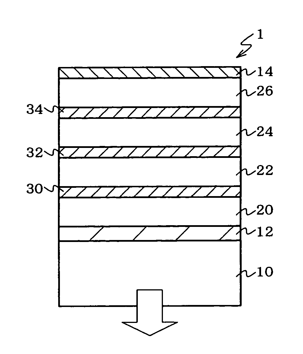
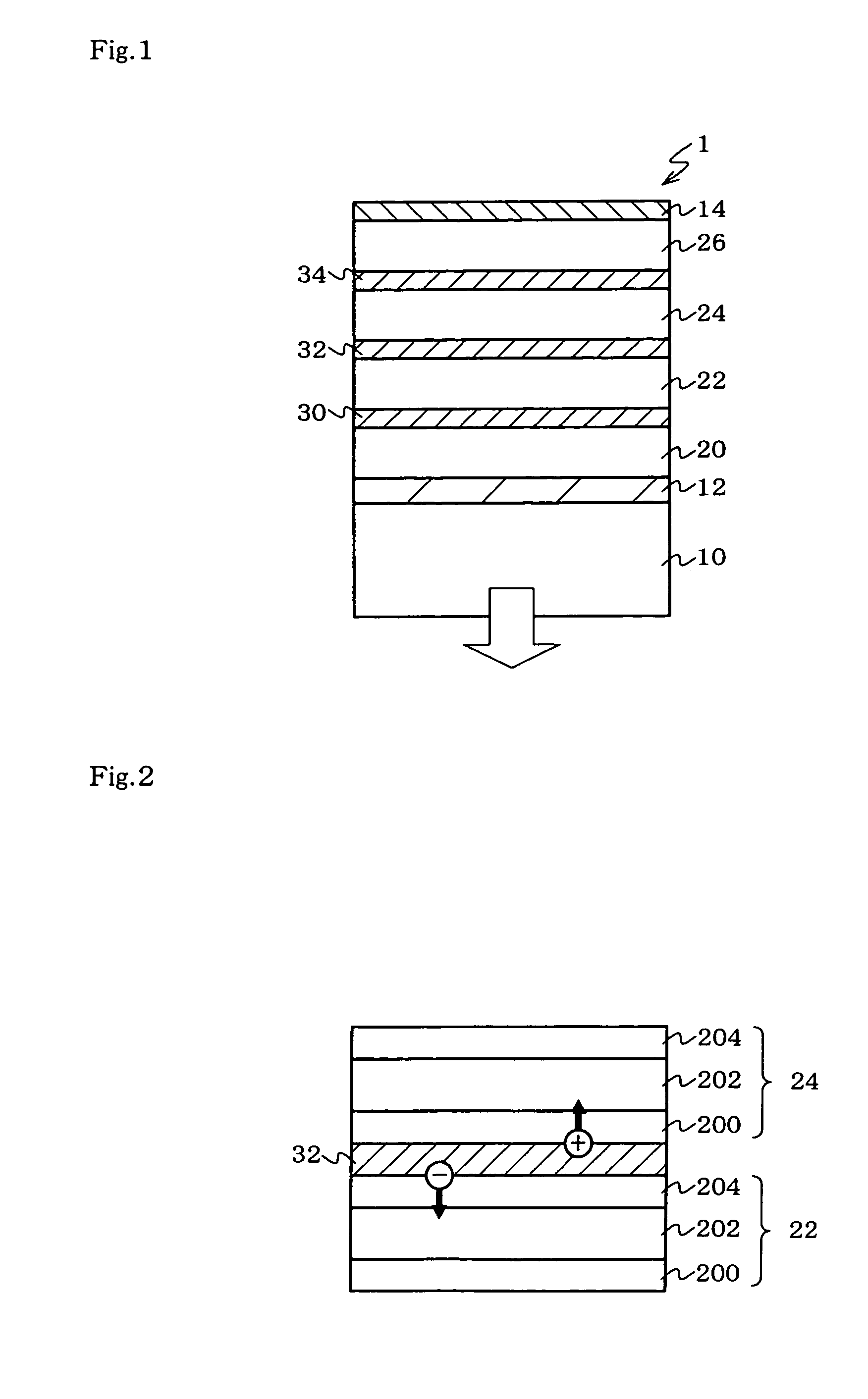
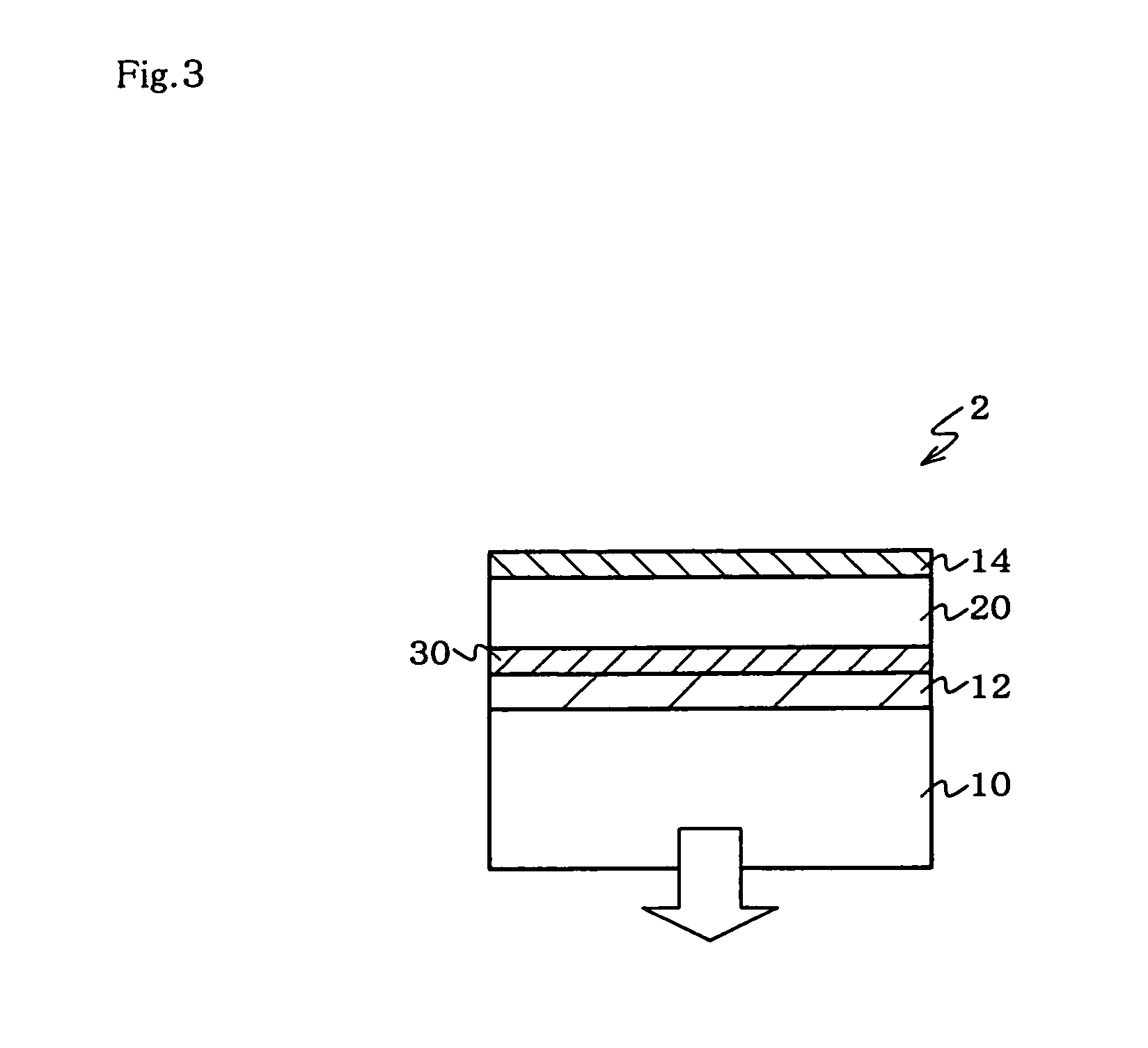
An organic EL device and a display with excellent viewing-angle properties and high efficiency are provided. An organic electroluminescent device (1) comprising: a transparent electrode (12), a counter electrode (14) arranged opposite to the transparent electrode (12), one or more intermediate conductive layers (30, 32 and 34) and one or more organic emitting layers (20, 22, 24 and 26) arranged between the transparent electrode (12) and the counter electrode (14), wherein the difference between na and nb is 0.2 or less when na is the refractive index of the intermediate conductive layer (30) and nb is the refractive index of the organic emitting layer (20).

Description

CLAIM OF PRIORITY[0001]This application claims priority under 35 USC 371 to International Application No. PCT / JP2004 / 005762, filed on Apr. 22, 2004, which claims priority to Japanese Patent Application No. 2003-119305, filed on Apr. 24, 2003, the entire contents of which are hereby incorporated by reference.TECHNICAL FIELD[0002]The invention relates to an organic electroluminescent device and display.BACKGROUND ART[0003]In order to make an organic electroluminescence (EL) device have a longer durability and higher efficiency, there is a technique of stacking a plurality of units, a unit being cathode / organic EL device / anode (for example, JP-A-H6-176870, JP-A-H11-312584 and JP-A-H11-312585).[0004]Such a device requires a lower current density than a device having one unit to obtain the same luminance. The device with plural units thus has a longer durability. However the technique has the following problem. An electrode must be extracted from an injection electrode arranged between a...

Claims


Application Information

Patent Timeline
Patent Type & Authority Patents(United States)
IPC IPC(8): H05B33/00H01L51/52H05B33/14H05B33/26
CPCH01L51/5265H01L51/5278H10K50/852H10K50/19H05B33/26H05B33/14
Inventor KUMA, HITOSHI
Owner IDEMITSU KOSAN CO LTD
Why Eureka
Try Eureka