Light-emitting device and method for manufacturing light-emitting device

a technology of light-emitting devices and manufacturing methods, which is applied in semiconductor devices, solid-state devices, diodes, etc., can solve the problems of poor injection balance, difficult to increase and improve the injection property of the hole, so as to improve the injection property and enhance the injection balance of the carrier. , the effect of improving the injection property

Inactive Publication Date: 2005-04-21
SEMICON ENERGY LAB CO LTD
View PDF32 Cites 77 Cited by
  • Summary
  • Abstract
  • Description
  • Claims
  • Application Information

AI Technical Summary

Benefits of technology

[0023] In the present invention, the hole-injecting property can be improved and the hole mobility can be enhanced by forming the barrier layer. As a result, the injection balance of the carrier can be enhanced and the internal quantum efficiency can be raised accordingly. Moreover, since the layer having the hole-transporting property is formed after removing the moisture a

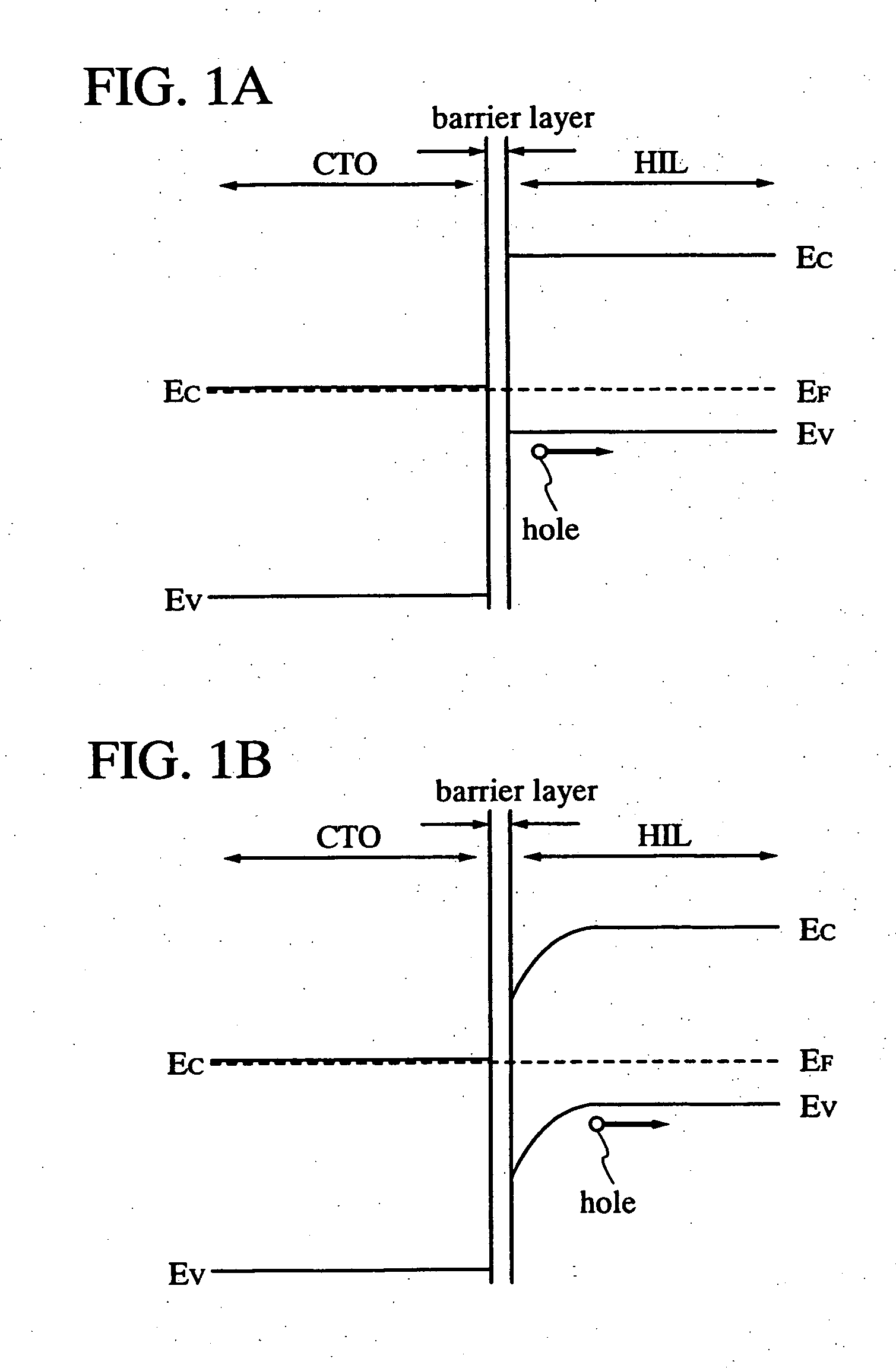
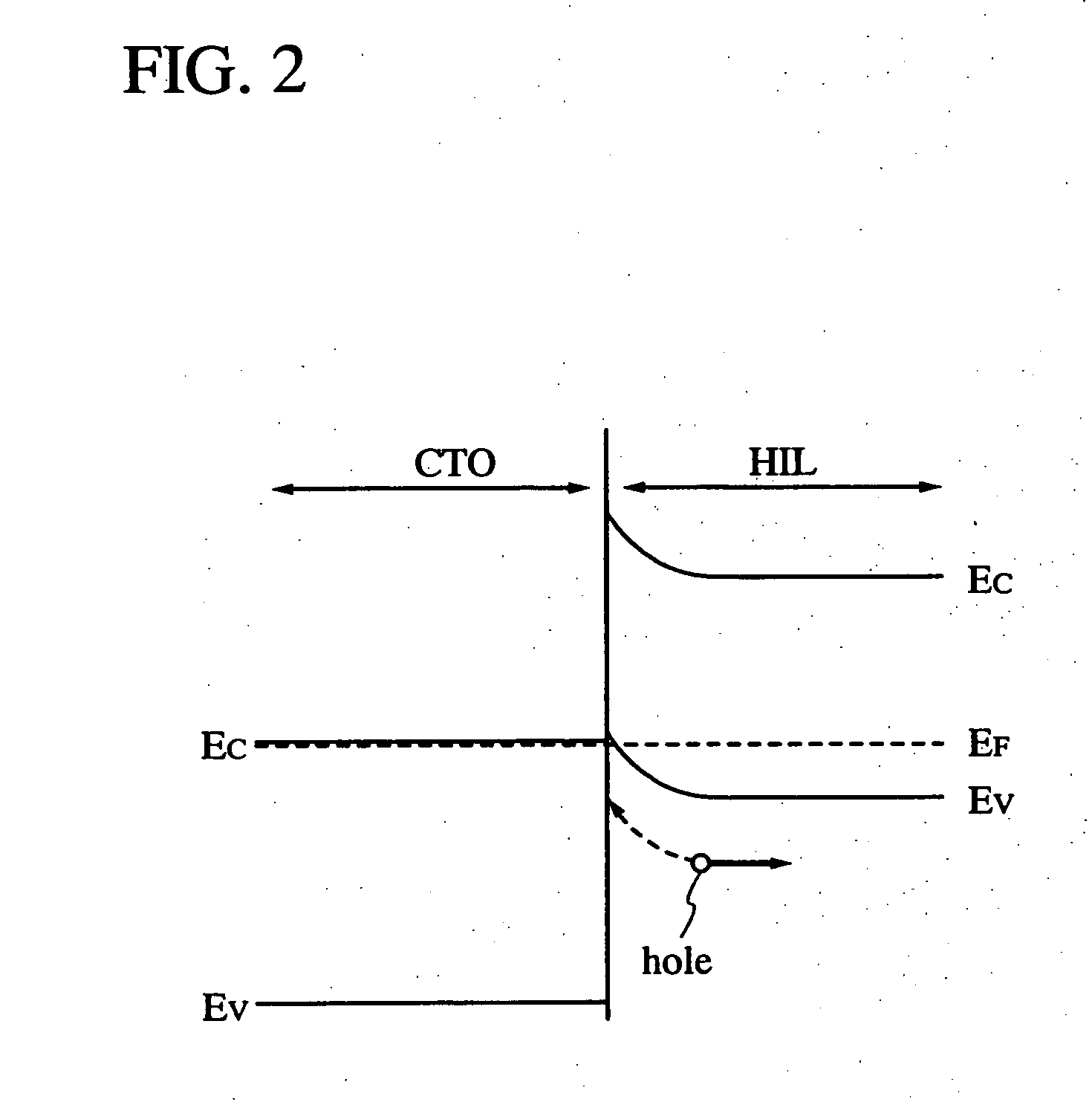
Problems solved by technology

As a result, the energy band of the hole-injecting layer or the hole-transporting layer bends, and this bend prevents the hole-injecting property from improving and causes the injection balance to become poor.
For this reason, it

Method used


Image

  • Light-emitting device and method for manufacturing light-emitting device
  • Light-emitting device and method for manufacturing light-emitting device
  • Light-emitting device and method for manufacturing light-emitting device

Examples


embodiment 1

[Embodiment 1]

[0097] The present embodiment explains an example of a pixel of the light-emitting device obtained by the manufacturing method of the present invention.

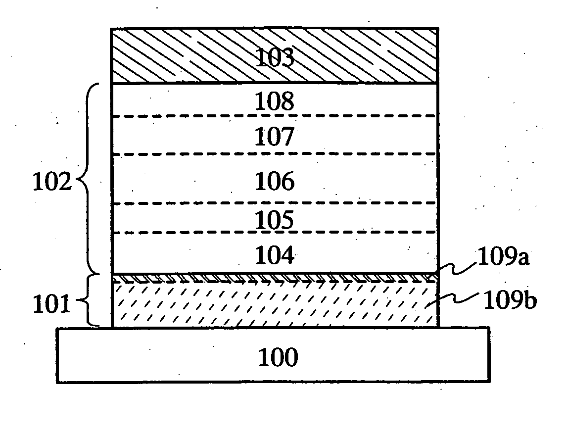
[0098]FIG. 8 is a cross-sectional view of the light-emitting device explained in the present embodiment. In FIG. 8, transistors 7001 to 7003 are formed over a substrate 7000. The transistors 7001 to 7003 are covered by a first interlayer insulating film 7004. Wirings 7005 to 7007 connecting with the transistors 7001 to 7003 through the contact hole are formed on the first interlayer insulating film 7004.

[0099] A second interlayer insulating film 7008 and a third interlayer insulating film 7009 are laminated over the first interlayer insulating film 7004 so as to cover the wirings 7005 to 7007. It is noted that the organic resin film, the inorganic insulating film, the insulating film including Si—O bond and Si—CHx bond made from the material selected from the siloxane group, or the like can be used as the material of ...

embodiment 2

[Embodiment 2]

[0111] This embodiment explains a circuit diagram of a pixel of a light-emitting device manufactured by the present invention with reference to FIGS. 9A to 9C. FIG. 9A is an equivalent circuit diagram of the pixel showing a signal line 6114, power supply lines 6115 and 6117, a scanning line 6116, a light-emitting element 6113, a TFT 6110 for controlling the input of a video signal into the pixel, a TFT 6111 for controlling the current value flowing between both electrodes of the light-emitting element 6113, and a capacitance element 6112 for holding the voltage between the gate and the source of the TFT 6111. Although FIG. 5B shows the capacitance element 6112, the capacitance element 6112 is not necessary when the gate capacitance of the TFT 6111 or another parasitic capacitance is enough.

[0112]FIG. 9B is a pixel circuit having the structure in which a TFT 6118 and a scanning line 6119 are newly provided in the pixel shown in FIG. 9A. The TFT 6118 makes it possible t...

embodiment 3

[Embodiment 3]

[0115] The present embodiment explains a structure of a light-emitting device manufactured by the present invention with reference to FIGS. 10A to 10F. FIG. 10A is a top view of the light-emitting device for explaining the concept of the light-emitting device having a pixel portion 6201, a signal line driver circuit 6202, and a scanning line driver circuit 6203 over a substrate 6200. A reference numeral 6204 denotes an input terminal for supplying power source potential or a signal to each circuit formed over the substrate 6200. Reference numerals 6205 to 6207 denote protective circuits for preventing the semiconductor element from being damaged due to the noise of the signal, the electrostatic, or the like. It is not always necessary to provide all the protective circuits 6205 to 6207 and any one or a plurality of protective circuits among them may be provided.

[0116] Although the signal line driver circuit 6202 and the scanning line driver circuit 6203 are formed ove...


PUM

PropertyMeasurementUnit
Densityaaaaaaaaaa
Electrical conductoraaaaaaaaaa
Lightaaaaaaaaaa

Abstract

It is an object of the present invention to provide a method for manufacturing a light-emitting device having high internal quantum efficiency, consuming less power, having high luminance, and having high reliability. The present invention provides a method for manufacturing a light-emitting device comprising the steps of forming a conductive light-transmitting oxide layer comprising a conductive light-transmitting oxide material and silicon oxide, forming a barrier layer in which density of the silicon oxide is higher than that in the conductive light-transmitting oxide layer over the conductive light-transmitting oxide layer, forming an anode having the conductive light-transmitting oxide layer and the barrier layer, heating the anode under a vacuum atmosphere, forming an electroluminescent layer over the heated anode, and forming a cathode over the electroluminescent layer, wherein the barrier layer is formed between the electroluminescent layer and the conductive light-transmitting oxide layer.

Description

1. FIELD OF THE INVENTION [0001] The present invention relates to a light-emitting device and to a method for manufacturing the light-emitting device, in which each pixel comprises a light-emitting element. 2. RELATED ART [0002] Since a light-emitting element emits light by itself, it is highly visible and does not require a backlight that is needed in a liquid crystal display device (LCD) and therefore the light-emitting element is best suited for a thin device. Moreover, the light-emitting element has a wider viewing angle than the LCD. For these reasons, attention has been paid to a light-emitting device using the light-emitting element as an alternative display device to a CRT and the LCD, and it has been tried to put the light-emitting device to practical use. An OLED (Organic Light Emitting Diode), which is one of the light-emitting elements, has an anode, a cathode, and a layer (hereinafter referred to as an electroluminescent layer) including an electroluminescent material w...

Claims


Application Information

Patent Timeline
IPC IPC(8): H01L21/00H01L27/32H01L51/50H01L51/52
CPCH01L27/322H01L27/3244H01L27/3276H01L51/5048H01L51/56H01L51/5092H01L51/52H01L51/5206H01L51/5237H01L51/5088H10K59/38H10K59/12H10K59/131H10K50/14H10K50/17H10K50/171H10K50/80H10K50/816H10K50/818H10K50/828H10K50/8426H10K50/846H10K50/844H10K50/81H10K71/00H10K50/84
Inventor YAMAZAKI, SHUNPEIAKIMOTO, KENGOSAKATA, JUNICHIROHIRAKATA, YOSHIHARUSONE, NORIHITO
Owner SEMICON ENERGY LAB CO LTD
Why Eureka
Try Eureka