In-series electrical connection of light-emitting nanowires

a technology of light-emitting nanowires and series connections, which is applied in the direction of electrical apparatus, semiconductor/solid-state device manufacturing, and semiconductor devices. it can solve the problems of connecting nanowires, and achieve the effect of no efficiency droop, good confinement of charge carriers

Active Publication Date: 2014-03-20
COMMISSARIAT A LENERGIE ATOMIQUE ET AUX ENERGIES ALTERNATIVES
View PDF11 Cites 29 Cited by
  • Summary
  • Abstract
  • Description
  • Claims
  • Application Information

AI Technical Summary

Benefits of technology

[0044]Then, since the device is based on nanowires, it is possible to obtain a good confinement of charge carriers while limiting their concentration, causing the “efficiency droop”, by an appropriate selection of the height of the nanowires, as will be explained in further detail hereafter.
[0045]Then, since the nanowires are not sensitive to the mesh parameter, the selection of the height of the nanowires, especially to obtain an appropriate current density with no efficiency droop, is decorrelated from the selection of the composition of the semiconductor forming the active area, for example, the indium composition in the case of a GaN-based device. There can thus be a wider choice for the emission wavelength. It is thus possible to manufacture LEDs based on nanowires emitting in the visible range, especially from blue to red in the case of a GaN-based LED, or even to form a LED emitting white light by varying the indium composition during the epitaxy of the nanowire core.
[0046]Further, since the active area forms most of the nanowire bulk, the device according to the invention has an improved internal quantum efficiency even with a strong injection current density.

Problems solved by technology

The main difficulty of connecting nanowires in series is the fact that the hole injection area and the electron injection area are arranged at opposite ends.

Method used


Image

  • In-series electrical connection of light-emitting nanowires
  • In-series electrical connection of light-emitting nanowires
  • In-series electrical connection of light-emitting nanowires

Examples


first embodiment

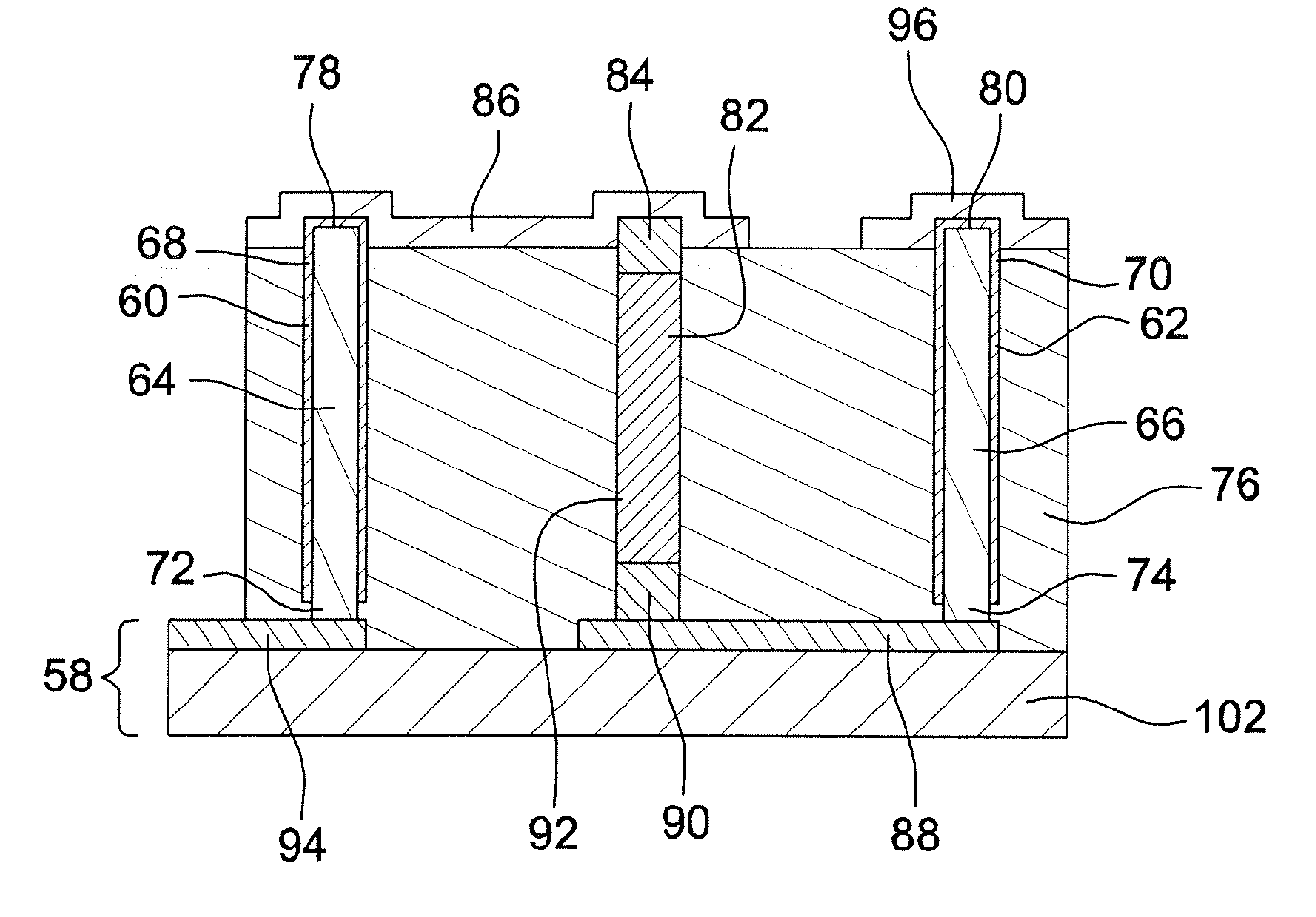
[0097] connection nanowire 82 is made of an electrically-conductive material. For example, connection nanowire 82 is metallic, which enables to obtain both a connection of high quality and a perfect compatibility with any type of nano-LED, whatever the materials and the structure of the hole and electron injection areas.

[0098]This however has the disadvantage of complicating the manufacturing process of an array of nano-LEDs since two types of manufacturing processes have to be provided, one for the nano-LEDs and the other for the connection nanowires.

second embodiment

[0099] the connection nanowire is a nano-LED which has then been modified be used as a connection nanowire. This enables to manufacture all the nanowires, nano-LEDs, and connection nanowires, during a same growth process.

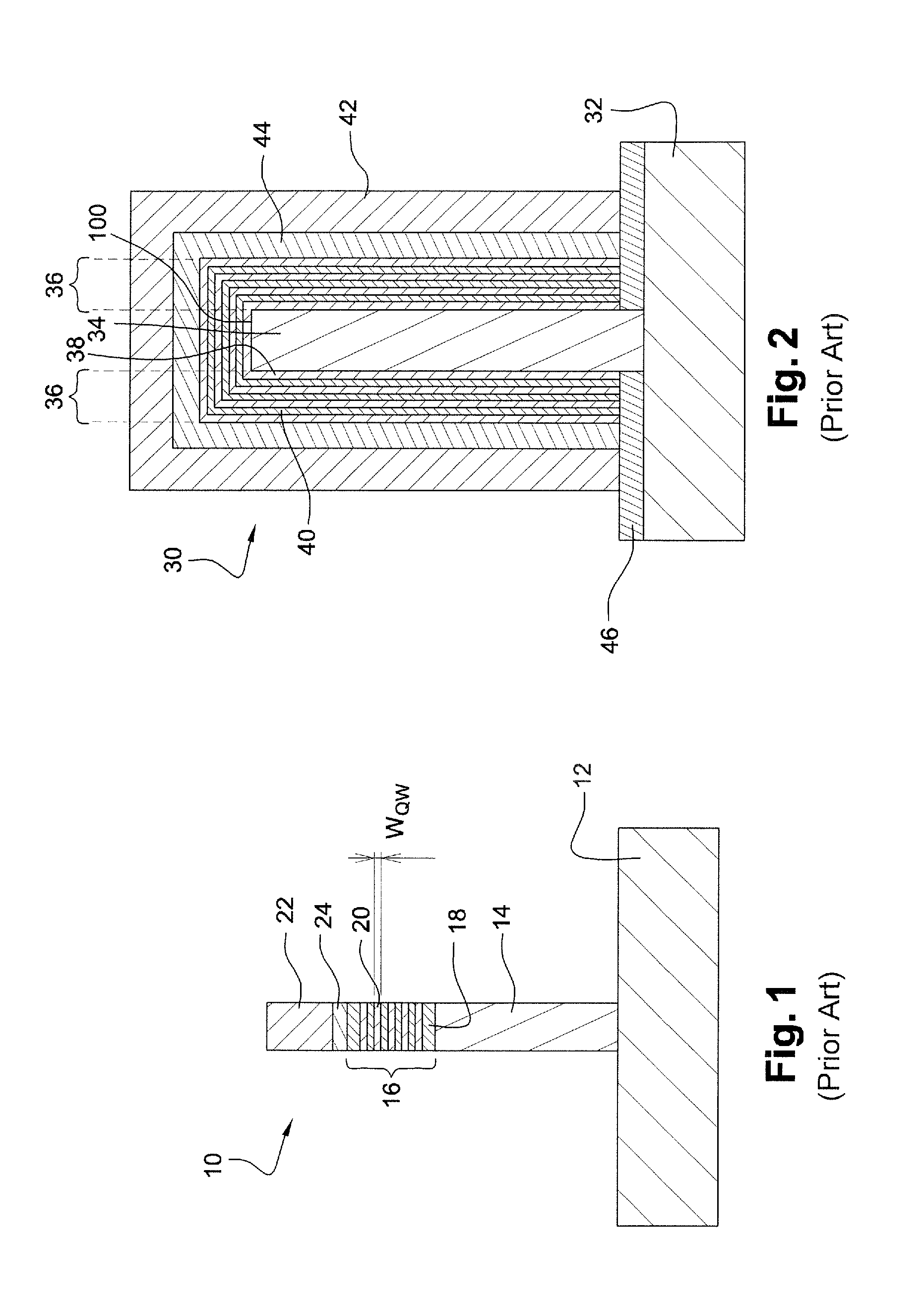
[0100]An application of the second embodiment to the core / shell nano-LEDs of FIG. 2 is now described in relation with FIGS. 6a, 6h, and 6c.

[0101]A nano-LED 30 is thus modified to remove a portion of shell 42 from head 84 thereof, and especially at least the portion of shell 42 covering upper surface 100 of core 34 of the nano-LED. This thus disengages core 34, which is electrically compatible with shell 42 forming a hole injection area of nano-LEDs 60, 62, and which is covered with first area 86 of the series connection, for example, a metal contact 86.

[0102]In the example illustrated in FIG. 6a, the top of nano-LED 30 has been removed to disengage core 34 while leaving in contact active area 36, as well as volumes 42 and 44, with conductive area 86.

[0103]In the ex...


PUM


Abstract

An optoelectronic device includes at least first and second light-emitting nanowires on a support, each comprising an area for the injection of holes and an area for the injection of electrons, a series electric connection including a connection nanowire on the support, which includes a first region forming an electric path with the hole injection area of the first nanowire, a second region forming an electric path with the electron injection area of the second nanowire, and a third region enabling a current to flow between first and second regions. Also included are a first conductive area connecting the hole injection area of the first nanowire and the first region of the connection nanowire and electrically insulated from the second nanowire, and a second conductive area connecting the second region of the connection nanowire and electron injection area of the second nanowire and electrically insulated from the first nanowire.

Description

FIELD OF THE INVENTION[0001]The invention relates to optoelectronic devices based on nanowires for the generation of light, and especially LEDs (light-emitting diodes).BACKGROUND[0002]Schematically, a LED comprises a semiconductor area for electron injection, a semiconductor area for hole injection, and a so-called “active” semiconductor area where the injected electrons and holes radiatively recombine.[0003]The first technology used to manufacture LEDs is the so-called “planar” technology. Because planar technology raises a number of issues, especially in terms of quantum efficiency and / or in terms of mesh matching between the different materials used and / or in terms of limitation of the wavelength capable of being emitted, LEDs based on nanowires having multiple quantum well confinement structures have been developed. Such nanowires, and more specifically their manufacturing method, indeed have a number of advantages, and in particular:[0004]a growth of nanowires on substrates, wi...

Claims


Application Information

Patent Timeline
Patent Type & Authority Applications(United States)
IPC IPC(8): H01L33/06H01L33/08
CPCH01L33/08H01L33/06H01L27/153H01L33/24H01L33/62H01L2924/0002H01L2924/00
Inventor BAVENCOVE, ANNE-LAUREGILET, PHILIPPEMOLLER, PIERRE
Owner COMMISSARIAT A LENERGIE ATOMIQUE ET AUX ENERGIES ALTERNATIVES
Why Eureka
Try Eureka