Semiconductor device and method for fabricating the same

Inactive Publication Date: 2008-02-28
PANASONIC CORP
View PDF9 Cites 29 Cited by
  • Summary
  • Abstract
  • Description
  • Claims
  • Application Information

AI Technical Summary

Benefits of technology

[0016]In the method for fabricating a semiconductor device of this invention, a semiconductor superlattice layer having concave-convex shapes can be easily formed. Furthermore, a semiconduct

Problems solved by technology

In a conventional nitride-based compound semiconductor LED, however, an expensive sapphire substrate with a small aperture is used for crystal growth, and hence, it is difficult t

Method used


Image

  • Semiconductor device and method for fabricating the same
  • Semiconductor device and method for fabricating the same
  • Semiconductor device and method for fabricating the same

Examples


embodiment 1

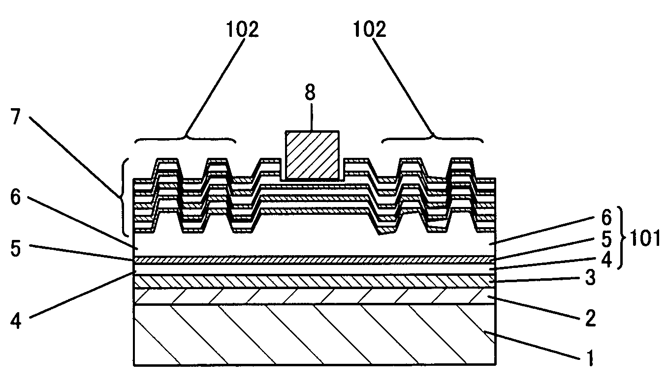
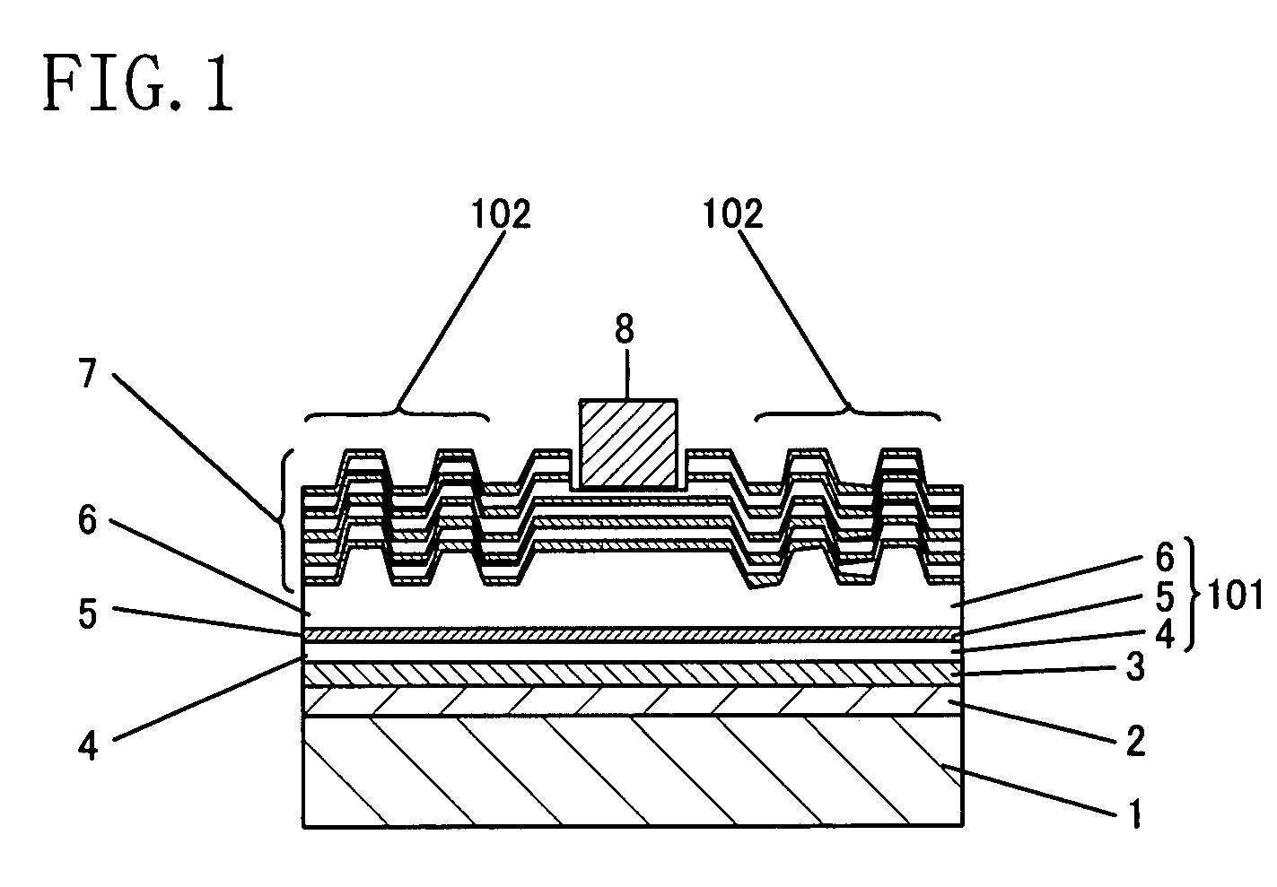
[0029]Embodiment 1 of the invention will now be described with reference to the accompanying drawings. FIG. 1 shows the cross-sectional structure of a semiconductor device according to Embodiment 1. As shown in FIG. 1, the semiconductor device of this embodiment is an LED. In the semiconductor device, a semiconductor multilayer 101 is bonded to a holding substrate 1 made of Si with a solder layer 2 and a P electrode 3, that is, a reflection electrode, sandwiched therebetween. A semiconductor superlattice layer 7 is formed on the semiconductor multilayer 101.

[0030]The solder layer 2 is preferably made of a material easily fused between metals, such as lead (Pb), tin (Sn), indium (In) or gold (Au). In this embodiment, a solder material utilizing eutectic of Sn and Au is used. As the P electrode 3 of this embodiment, a multilayered film of palladium (Pd), platinum (Pt) and gold (Au) is used. In this case, reflectance of light of a wavelength of 450 nm entering the interface between GaN...

embodiment 2

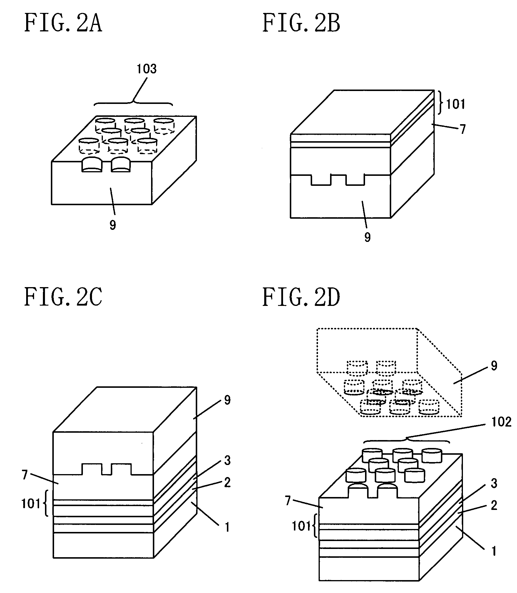
[0056]Embodiment 2 of the invention will now be described with reference to the accompanying drawing. FIG. 10 is a cross-sectional view of a semiconductor device according to Embodiment 2. As shown in FIG. 10, the semiconductor device of this embodiment is a semiconductor laser diode. In this semiconductor device, a semiconductor superlattice layer 7 and a semiconductor multilayer 101 are successively formed on a crystal growing substrate 9 of n-type Si.

[0057]The crystal growing substrate 9 has a one-dimensional periodic structure in the form of periodically formed recesses. As the one-dimensional periodic structure, recesses with a depth of 5 μm may be formed, for example. In the semiconductor device of this embodiment, there is no need to form a photonic crystal by a semiconductor superlattice layer 7. When the width at the inclined part (a step portion 41) of each recess is set equal to or larger than a part serving as a waveguide (with a width of approximately 2 μm), such as a r...

embodiment 3

[0062]Embodiment 3 of the invention will now be described with reference to the accompanying drawing. FIG. 11 is a cross-sectional view of a semiconductor device according to Embodiment 3. As shown in FIG. 11, the semiconductor device of this embodiment is a field effect transistor. In this semiconductor device, a semiconductor superlattice layer 7 and a semiconductor multilayer 101 are successively formed on a crystal growing substrate 9 made of n-type Si.

[0063]The crystal growing substrate 9 has a one-dimensional periodic structure in the form of periodically formed recesses. As the one-dimensional periodic structure, recesses with a depth of 200 nm may be formed, for example. In the semiconductor device of this embodiment, there is no need to form a photonic crystal by a semiconductor superlattice layer 7. When the width at the inclined part (a step portion 41) of each recess is set equal to or larger than the gate length (approximately 0.1 to 1 μm) in the field effect transistor...


PUM


Abstract

A semiconductor device includes a semiconductor superlattice layer and a semiconductor multilayer. The semiconductor superlattice layer has periodic concave-convex shapes, and a plurality of semiconductor films each having bent portions in accordance with the concave-convex shapes are stacked in the semiconductor superlattice layer. The semiconductor multilayer is formed so as to cover the concave-convex shapes and includes an active layer.

Description

CROSS-REFERENCE TO RELATED APPLICATIONS[0001]This application claims priority under 35 U.S.C. §119 on Patent Application No. 2006-230405 filed in Japan on Aug. 28, 2006, the entire contents of which are hereby incorporated by reference.BACKGROUND OF THE INVENTION[0002]The present invention relates to a semiconductor device and a method for fabricating the same, and more particularly, it relates to a semiconductor device such as a semiconductor light emitting diode, a semiconductor laser diode, a bipolar transistor or a field effect transistor.[0003]It has been conventionally difficult to attain high luminous efficiency in light emitting devices such as a light emitting diode (LED) and a semiconductor laser diode for emitting light of a wavelength band from ultraviolet light to blue or green light, but these light emitting devices are now being earnestly studied and developed by using nitride-based compound semiconductors typified by GaN. In particular, since an LED is more easily fa...

Claims


Application Information

Patent Timeline
IPC IPC(8): H01L29/06H01L21/00H01L33/06H01L33/32H01L33/40
CPCH01L29/0657H01L29/0684H01L29/155H01L2933/0083H01L29/7787H01L33/04H01L33/20H01L29/2003
Inventor ORITA, KENJIFUKUSHIMA, YASUYUKI
Owner PANASONIC CORP
Why Eureka
Try Eureka