
Blue LED epitaxial structure with suppression polarization effect barrier layer

A polarization effect and epitaxial structure technology, applied in the direction of electrical components, circuits, semiconductor devices, etc., can solve problems such as limited effects, achieve the effects of suppressing overflow, improving crystal quality, and suppressing polarization

Active Publication Date: 2016-05-04
NANTONG TONGFANG SEMICON
View PDF6 Cites 28 Cited by
  • Summary
  • Abstract
  • Description
  • Claims
  • Application Information

AI Technical Summary

Problems solved by technology

Limit the overflow of carriers and improve the ability of uniform distribution of holes, that is, increase the recombination probability of the wave function, but the effect is limited

Method used


Image

  • Blue LED epitaxial structure with suppression polarization effect barrier layer
  • Blue LED epitaxial structure with suppression polarization effect barrier layer
  • Blue LED epitaxial structure with suppression polarization effect barrier layer

Examples


Embodiment 1

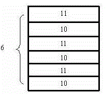
[0060] The barrier layer 6 for suppressing the polarization effect is grown for 3 cycles in nitrogen, hydrogen or a hydrogen-nitrogen mixed environment.

[0061] ①Grow Al first x Ga 1-x The N layer 10 was grown at a temperature of 700° C., the growth pressure was 300 mbar, and the thickness was 50 nm; the SiN layer 11 was regrown at a growth temperature of 700° C., the growth pressure was 300 mbar, and the thickness was 50 nm.

[0062] ② Second, grow Al x Ga 1-x The N layer 10 is grown at a temperature of 700° C., the growth pressure is 300 mbar, and the thickness is 75 nm; the SiN layer 11 is regrown at a growth temperature of 700° C., the growth pressure is 300 mbar, and the thickness is 40 nm.

[0063] ③Secondary growth of Al x Ga 1-x The N layer 10 is grown at a temperature of 700° C., the growth pressure is 300 mbar, and the thickness is 100 nm; the SiN layer 11 is regrown at a growth temperature of 700° C., the growth pressure is 300 mbar, and the thickness is 30 nm...

Embodiment 2

[0065] The barrier layer 6 for suppressing the polarization effect is grown for 3 cycles in nitrogen, hydrogen or a hydrogen-nitrogen mixed environment.

[0066] ①Grow Al first x Ga 1-x The N layer 10 is grown at a temperature of 800° C., the growth pressure is 300 mbar, and the thickness is 50 nm; the SiN layer 11 is regrown at a growth temperature of 800° C., the growth pressure is 300 mbar, and the thickness is 50 nm.

[0067] ② Second, grow Al x Ga 1-x The N layer 10 is grown at a temperature of 800° C., the growth pressure is 300 mbar, and the thickness is 75 nm; the SiN layer 11 is regrown at a growth temperature of 800° C., the growth pressure is 300 mbar, and the thickness is 40 nm.

[0068] ③Secondary growth of Al x Ga 1-x The N layer 10 is grown at a temperature of 800° C., the growth pressure is 300 mbar, and the thickness is 100 nm; the SiN layer 11 is regrown at a growth temperature of 800° C., the growth pressure is 300 mbar, and the thickness is 30 nm.

Embodiment 3

[0070] The barrier layer 6 for suppressing the polarization effect is grown for 3 cycles in nitrogen, hydrogen or a hydrogen-nitrogen mixed environment.

[0071] ①Grow Al first x Ga 1-x The N layer 10 is grown at a temperature of 900° C., the growth pressure is 300 mbar, and the thickness is 50 nm; the SiN layer 11 is regrown at a growth temperature of 900° C., the growth pressure is 300 mbar, and the thickness is 50 nm.

[0072] ② Second, grow Al x Ga 1-x The N layer 10 was grown at a temperature of 900° C., the growth pressure was 300 mbar, and the thickness was 75 nm; the SiN layer 11 was regrown at a growth temperature of 900° C., the growth pressure was 300 mbar, and the thickness was 40 nm.

[0073] ③Secondary growth of Al x Ga 1-x The N layer 10 is grown at a temperature of 900° C., the growth pressure is 300 mbar, and the thickness is 100 nm; the SiN layer 11 is regrown at a growth temperature of 900° C., the growth pressure is 300 mbar, and the thickness is 30 nm...


PUM


Abstract

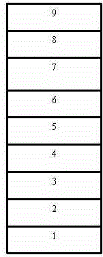
The invention provides a blue LED epitaxial structure with a suppression polarization effect barrier layer, and relates to the technical field of light emitting diodes. The blue LED epitaxial structure comprises a substrate, an AlN buffer layer, a U-type GaN layer, an N-type GaN layer, a shallow quantum well layer, an active region, an electron blocking layer, and a P-type GaN layer in sequence from bottom to top, the suppression polarization effect barrier layer is inserted between the shallow quantum well layer and the active region, and the suppression polarization effect barrier layer comprises an AlxGal-xN layer and a SiN layer from bottom to top. According to the blue LED epitaxial structure, a novel barrier layer is inserted into the conventional epitaxial structure, the stress is released, polarization is suppressed, the defect density is reduced, the radiative recombination probability is improved, the polarization effect is reduced, and the quantum efficiency in the LED is improved.

Description

technical field [0001] The invention relates to the technical field of light-emitting diodes, in particular to an epitaxial structure and a growth method of a blue-light LED with a polarization-effect-suppressing barrier layer. Background technique [0002] With the increasing application of blue GaN-based LEDs, people pay more attention to the brightness of blue GaN-based LEDs. In recent years, LED researchers have adjusted the patterned substrate specifications, increased injection current expansion, suppressed polarization effects, and improved crystal quality. , Increase the hole doping concentration, etc. to obtain high-brightness epitaxial wafers. [0003] Due to the lattice mismatch between the sapphire substrate and the GaN material in the traditional blue-light GaN-based LED epitaxial structure and growth method, spontaneous polarization and piezoelectric polarization result in spatial separation of the wave functions of electrons and holes in the quantum well, ther...

Claims


Application Information

Patent Timeline
Patent Type & Authority Applications(China)
IPC IPC(8): H01L33/12H01L33/14H01L33/06H01L33/00
Inventor 田宇张晓龙俞登永郑建钦曾欣尧童敬文吴东海李鹏飞
Owner NANTONG TONGFANG SEMICON
Learn More