Semiconductor ultraviolet source device

An ultraviolet light source and semiconductor technology, applied in the direction of semiconductor devices, electrical components, circuits, etc., can solve the problems of low LED luminous efficiency, achieve the effect of improving luminous efficiency, eliminating tilt effect, and improving internal quantum efficiency IQE

Active Publication Date: 2013-08-14
QINGDAO JASON ELECTRIC
View PDF7 Cites 28 Cited by
  • Summary
  • Abstract
  • Description
  • Claims
  • Application Information

AI Technical Summary

Problems solved by technology

[0006] Aiming at the problem of low luminous efficiency of existing LEDs, the present invention proposes a semiconductor ultraviolet light source device, which is realized by the following technical scheme:

Method used


Image

  • Semiconductor ultraviolet source device
  • Semiconductor ultraviolet source device
  • Semiconductor ultraviolet source device

Examples


Embodiment 1

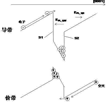
[0032] Embodiment 1, in order to facilitate processing, the epitaxial material of the semiconductor ultraviolet light source device in this embodiment is group III nitride of wurtzite structure, and the main epitaxial growth plane of the epitaxial structure of the device is the (0001) plane.

[0033] The ultraviolet LED of this embodiment is formed on the substrate 10 (see Figure 4), the substrate 10 may be a suitable substrate material such as silicon (eg Si), sapphire (eg c-plane sapphire or c-plane patterned sapphire), AlN, GaN or AlGaN. An epitaxial substrate 20 is formed on the substrate 10, preferably an epitaxial AlN epitaxial layer, or an AlGaN epitaxial layer with a high Al composition. The thickness of the epitaxial substrate 20 is preferably 100 nm to 3 μm. Above the epitaxial substrate is an electron supplying layer 40 N-type AlGaN with a thickness of at least 2 μm in order to have good electrical conductivity and material quality. In order to improve the materi...

Embodiment 2

[0037] The difference between the second embodiment and the first embodiment is that the Al composition of the electron supply layer 40 in this embodiment is higher than the Al composition of the quantum barrier 552 or the average Al composition of the quantum barrier, such as the N-type electron supply layer. The aluminum composition of 40 is 1.1 to 1.2 times that of the quantum barrier. In this way, it is convenient to apply in-plane biaxial compressive stress to the quantum barrier, causing the piezoelectric polarization electric field to partially offset the self-polarization electric field, and facilitating the transport of electrons and holes to the quantum well.

Embodiment 3

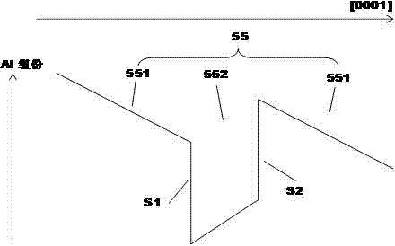
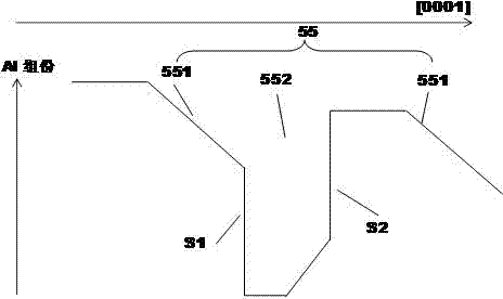
[0038] Embodiment 3: The AlINGaN ultraviolet LED epitaxially formed along the c direction in this embodiment has a light-emitting region composed of AlInGaN / AlInGaN multiple quantum wells, wherein the Al composition of the quantum barrier is x Al-QB refer to Figure 2-2 , the component gradient along the c direction satisfies:

[0039] when hour, , that is: in the first half of the barrier, the aluminum composition gradient of the quantum barrier along the epitaxial growth direction is zero;

[0040] when hour, , in the second half of the barrier, the aluminum composition gradient of the quantum barrier along the epitaxial growth direction ranges from -0.1% / nm to -2% / nm;

[0041] And the Al composition of the quantum well, x Al-QW , the component gradient along the c direction satisfies:

[0042] when hour, , that is: in the first half of the well, the aluminum composition gradient of the quantum well along the epitaxial growth direction is zero;

[0043] when...


PUM


Abstract

The invention provides a semiconductor ultraviolet source device. A quantum well and a quantum barrier in the epitaxial growth structure of the device have component gradients in the epitaxial growth direction, and the directions of the component gradients of the quantum well and the quantum barrier in the epitaxial growth direction are opposite. Heterostructures such as the energy band structures of multiple quantum wells are regulated through using the variation of the Al (aluminum) component of AlInGaN material, the energy band edge inclination of the quantum well and the quantum barrier is reduced, electrons and holes injected to the barrier are reduced, the positive working voltage of an ultraviolet LED (light emitting diode) is reduced, and the light emitting efficiency of the quantum well is improved.

Description

technical field [0001] The invention relates to the field of semiconductor devices, in particular to an epitaxial structure of a semiconductor solid-state ultraviolet light source device. Background technique [0002] The band width of group III nitride AlInGaN material is continuously adjustable from 0.7 eV to 6.2 eV, and it is the main material system for making semiconductor solid-state ultraviolet light-emitting diodes (LEDs). Compared with traditional UV light sources, AlInGaN semiconductor UV LEDs have many advantages, such as pollution-free, small size, long life, high efficiency, fast response, adjustable wavelength, high optical power density, and flexible application product design. important role. High-power 365 nm LEDs are expected to replace high-pressure mercury lamps (I2 line, 365 nm) as the next generation of high-efficiency UV curing light sources; high-power deep UV LEDs (wavelength < 290 nm) will definitely replace low-pressure mercury lamps (253.7 nm ...

Claims


Application Information

Patent Timeline
Patent Type & Authority Applications(China)
IPC IPC(8): H01L33/06H01L33/32
CPCH01L33/0025H01L33/32H01L33/06
Inventor 张剑平高英
Owner QINGDAO JASON ELECTRIC
Why Eureka
Try Eureka