Optical navigation sensor with integrated lens

a technology of optical navigation sensor and integrated lens, which is applied in the direction of instruments, static indicating devices, counting objects on conveyors, etc., can solve problems such as intermittent failure of sensors, and achieve the effect of optimizing generation and capture of reflected images, reducing the number of individual components

Inactive Publication Date: 2005-11-22
SAMSUNG ELECTRONICS CO LTD
View PDF2 Cites 79 Cited by
  • Summary
  • Abstract
  • Description
  • Claims
  • Application Information

AI Technical Summary

Benefits of technology

[0015]An optical navigation sensor apparatus according to the invention provides a number of advantages over prior devices, including: elimination of the need for covering the hole in the aperture plate with the piece of tape; a significant reduction in the number of individual component parts that must be handled; and automatically alignment some or all of the components of the optical navigation apparatus in a proper orientation to optimize generation and capture of the reflected image.

Problems solved by technology

Dust in the sensor 18 can cause intermittent failures of the sensor 18, as the dust moves around inside the sensor 18 and interferes with transmission of the reflected image to the electronic chip 12.

Method used


Image

  • Optical navigation sensor with integrated lens
  • Optical navigation sensor with integrated lens
  • Optical navigation sensor with integrated lens

Examples


Embodiment Construction

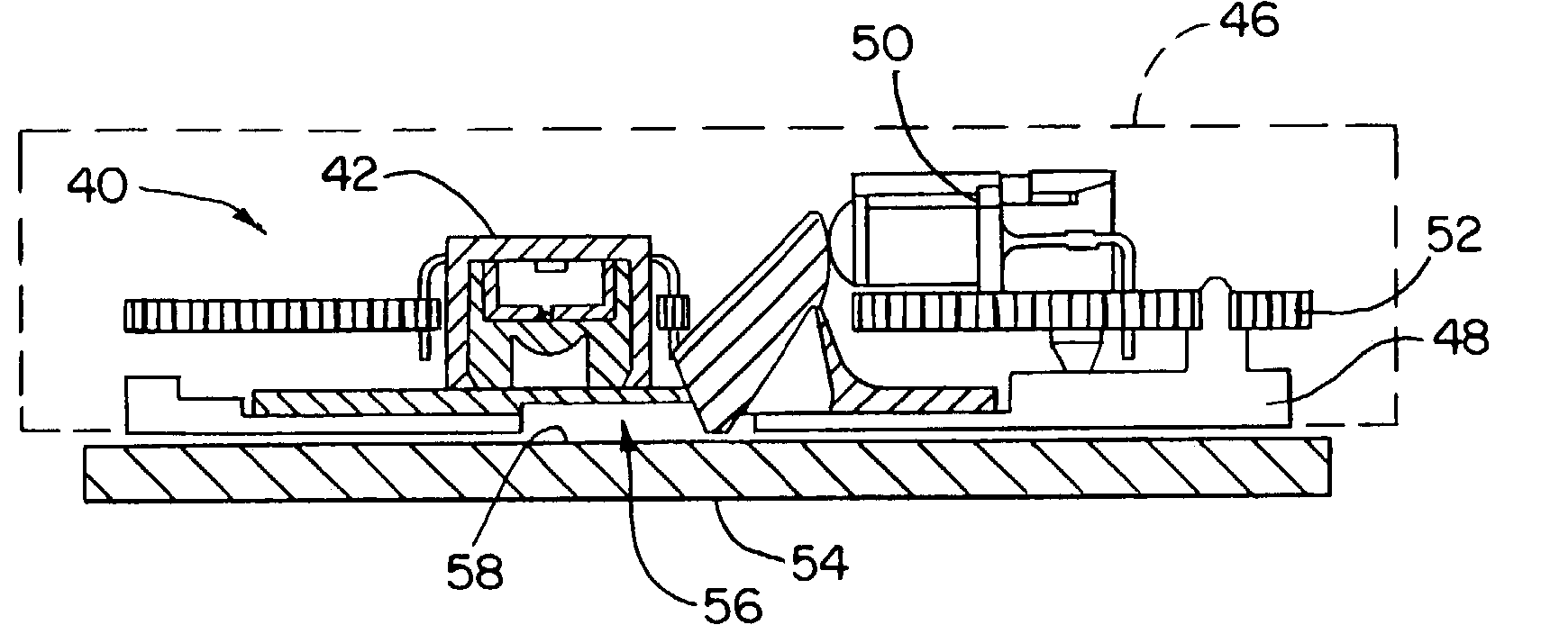
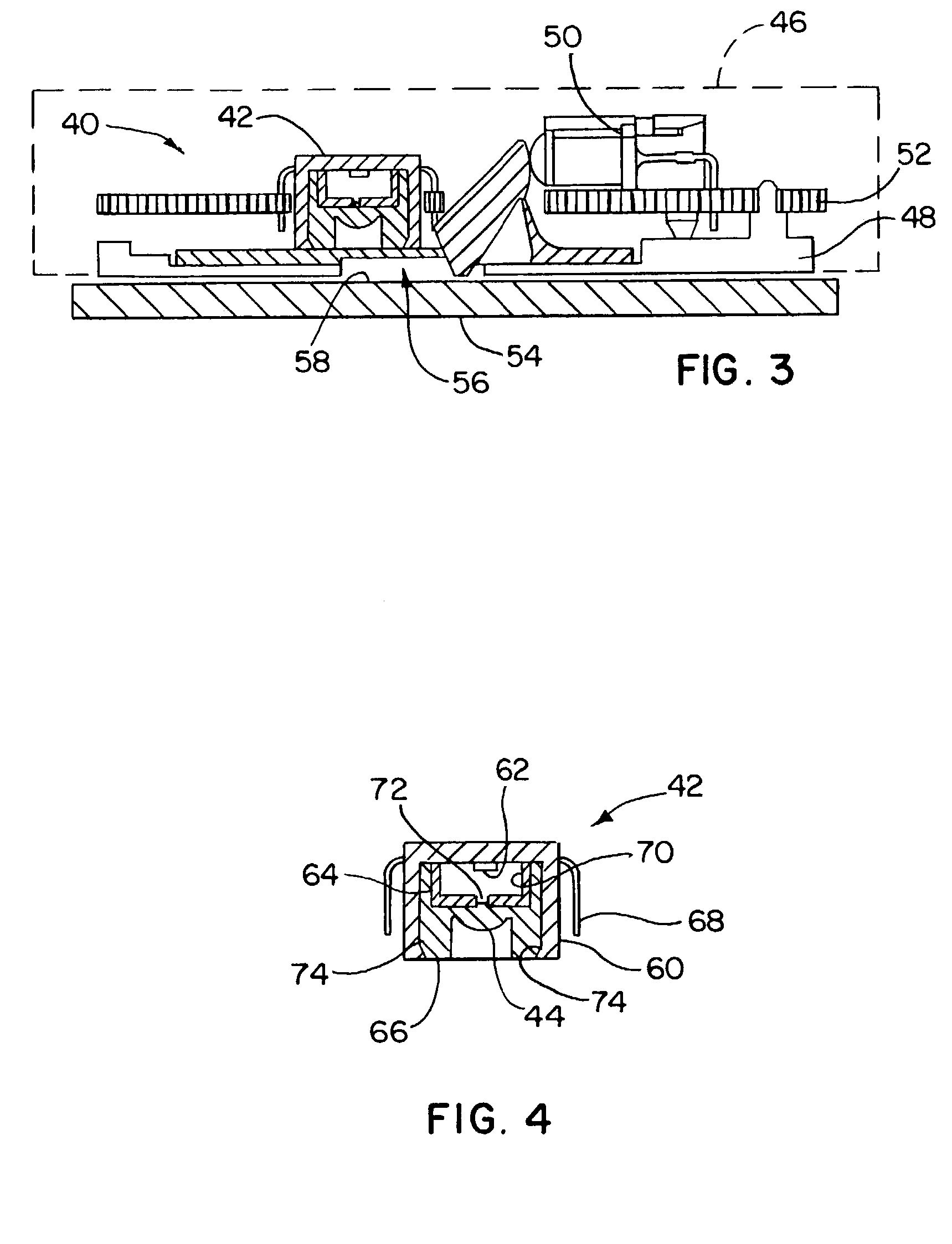
[0023]FIGS. 3, 4 and 5 show a first exemplary embodiment of an optical navigation sensor apparatus 40 including an optical sensor 42 having an integral imaging lens 44, according to the invention, in an optical computer mouse 46. The optical navigation sensor apparatus 40 is operatively attached, in a manner described in greater detail below, to a base plate 48 of the optical mouse 46.

[0024]The optical sensor navigation apparatus 40 of the first exemplary embodiment includes the optical navigation sensor 42, and an LED 50 operatively connected to a circuit board 52 mounted on the base plate 48, and a collimating lens 54 for directing light from the LED 50 through a hole 56 in the base plate 48 to illuminate a small area of a surface 58 beneath the base plate 48.

[0025]The optical navigation sensor 42 includes a sensor housing 60, an electrical chip in the form of a die 62, an aperture housing 64, and an imaging lens housing 66. The sensor housing 60 is an insert molded lead frame, ha...


PUM


Abstract

An optical navigation sensor apparatus for an optical mouse includes an optical navigation sensor having an electronic chip, an aperture plate and an imaging lens integrated into a single package. The imaging lens includes a lens housing surrounding the aperture and providing a barrier to the entry of foreign matter into the aperture. In one form, the optical navigation sensor also includes a light emitting diode (LED) for illuminating a small area of a surface under the sensor and generating a reflected image that is detected by the electronic chip. In a sensor having an integral LED, an integral collimating lens is included for receiving light from the LED and focusing the light from the LED on the surface to be illuminated. The collimating lens is incorporated into a lens housing surrounding the LED and protecting the LED from exposure to foreign material.

Description

TECHNICAL FIELD OF THE INVENTION[0001]This invention relates an optical navigation sensor apparatus, and more particularly to an optical navigation sensor that is particularly well suited for use in an optical navigation sensor apparatus of an optical computer mouse.BACKGROUND OF THE INVENTION[0002]An optical computer mouse typically includes an optical navigation sensor apparatus, having a number of separate components, including an electronic chip that functions as a miniature digital camera to continually record images of a surface that the mouse is resting upon, and determine the speed and direction that the mouse is being moved across the surface by comparing sequentially recorded images of the surface. The images are recorded at a very high rate, such as 1500 images per second, and the resolution of the sensor is high, so that very small movements of the mouse can be detected.[0003]The optical navigation sensor apparatus typically includes a light source, in the form of a ligh...

Claims


Application Information

Patent Timeline
Patent Type & Authority Patents(United States)
IPC IPC(8): G06M7/00G06F3/033H01J40/14H01J3/00H01J40/00H01J3/14H01L31/12G06F3/0354G06F3/03
CPCG06F3/0317
Inventor LEONG, AK WINGSINGH, GURBIRLYE, POH HUATLEE, SAI MUN
Owner SAMSUNG ELECTRONICS CO LTD
Why Eureka
Try Eureka