Functional-pattern management system for device verification

a technology of functional pattern management and device verification, applied in error detection/correction, instruments, computing, etc., can solve the problems of large verification challenge, almost always impractical, and huge expense, and achieve the effect of better understanding by users and better coverag

Inactive Publication Date: 2005-11-22
BELL SEMICON LLC
View PDF12 Cites 20 Cited by
  • Summary
  • Abstract
  • Description
  • Claims
  • Application Information

AI Technical Summary

Benefits of technology

[0014]Accordingly, there is provided herein a system and method for verifying the functionality of a device design. In one embodiment, the system includes a profile generation module, a coverage measurement module, and a pattern generation module. The profile generation module operates from a rule set that represents the design specification and any applicable standards, and a profile mode that specifies “interesting” aspects of test patterns for device design verification. The interesting aspects are determined by the user and may be somewhat subjective, although it is preferable that the aspects relate to the coverage provided by the test pattern. Given the rule set and the profile mode, the profile generation module determines an ordered set of variable values that at least partially specify a test pattern, and produces a profile that intelligibly describes the interesting aspects of the test pattern. Tools such as the coverage measurement module and the pattern generation module may then operate on the profile of the test pattern. The coverage measurement module analyzes the profile to determine coverage, and the analysis results may be operated on by the profile generation module to determine a profile for an improved test pattern. The coverage measurement module may preferably employ a design-vector grading (DVG) metric or a variation thereof. The pattern generation module converts the profile into a test pattern having the interesting aspects specified in the profile. The system may further include a pattern profiling module for converting existing test patterns into profiles, and a pattern checking module for verifying that profile-represented patterns satisfy particular rules. This system efficiently produces test patterns that are better understood by the user and that enable better coverage due to the use of the human-intelligible profile.

Problems solved by technology

As technology continues to improve, digital electronic products become increasingly sophisticated and present a bigger verification challenge to product designers.
A huge expense is incurred in setting up the manufacturing process for constructing a particular product, so designers need to be sure their product design operates correctly before finally implementing it in silicon.
This is almost always impractical due to the number of valid sets of input signals, particularly in the case of devices with a large number of internal states, e.g. microprocessors.
These questions are still the subject of much debate.
This method is undirected and results in inefficient use of computer resources.
It should be noted that while complete verification implies complete coverage of any given device design aspect, the converse is not necessarily true.
However, since a single HDL code line can often represent a circuit module of moderate complexity, a single execution of that code line falls well short of thoroughly verifying that code module.
Again, this falls well short of thoroughly verifying the device since most of the combinations of nodes states go untested.
While effective, this measurement method is statistical in nature and requires a substantial amount of computer resources.
Test patterns can comprise an enormous amount of data, in fact the running of some test patterns can last for days.
Construction and handling of these test patterns can be difficult and unwieldy.

Method used


Image

  • Functional-pattern management system for device verification
  • Functional-pattern management system for device verification
  • Functional-pattern management system for device verification

Examples


Embodiment Construction

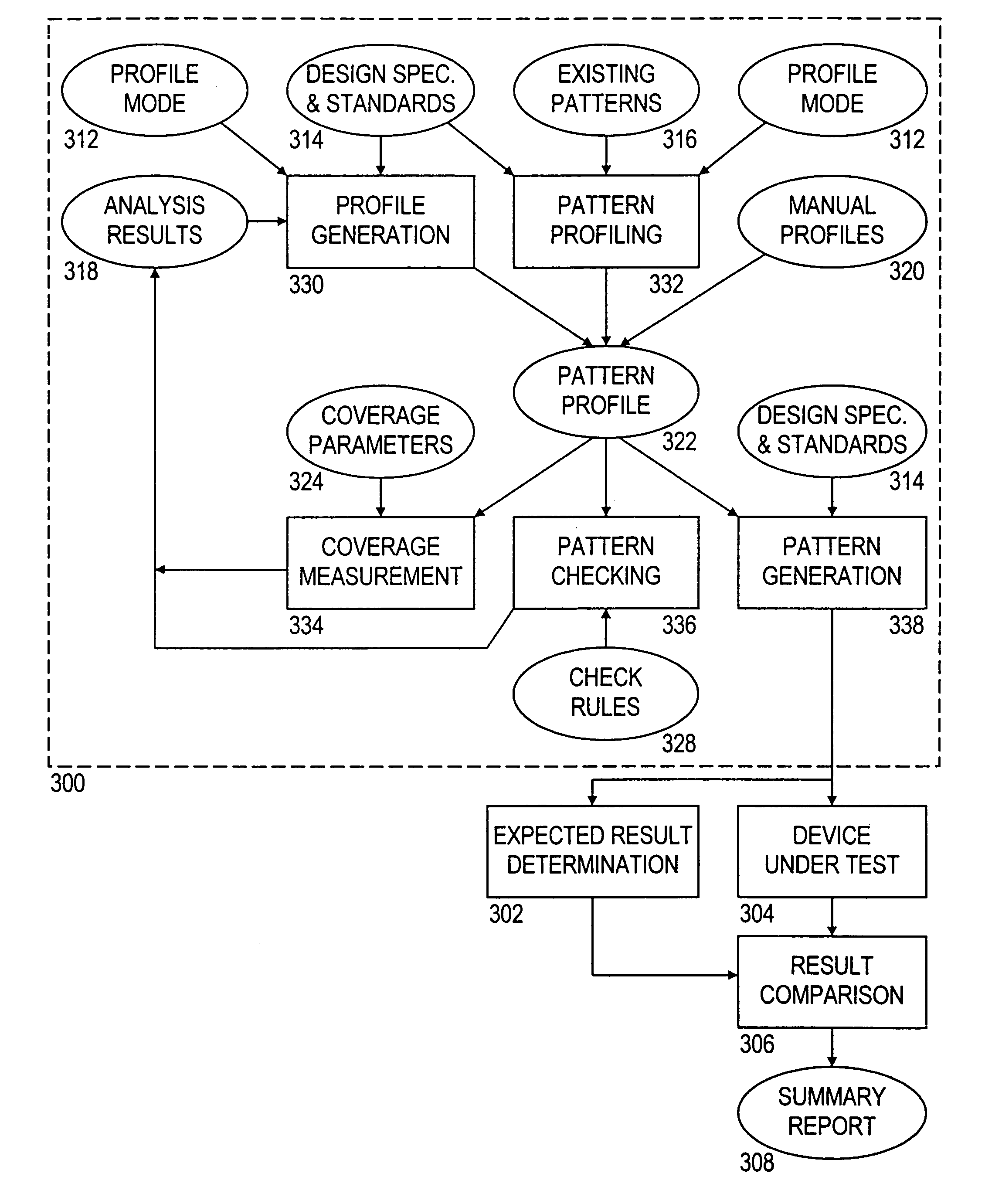
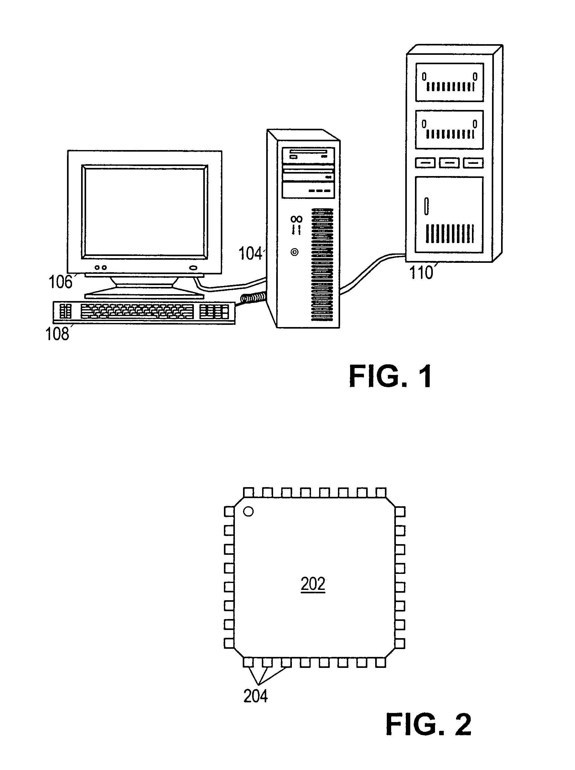
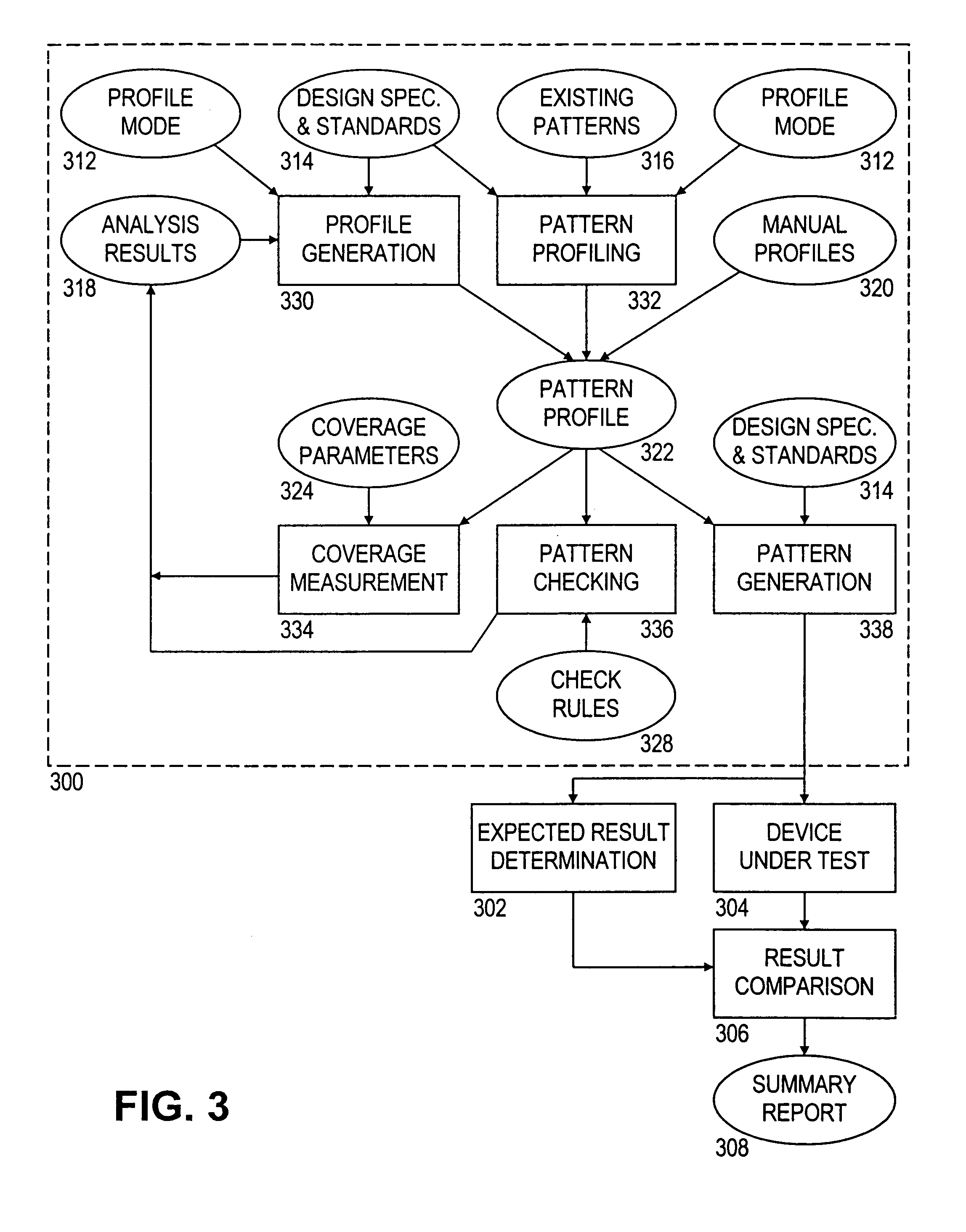
[0021]Turning now to the figures, FIG. 1 shows a system for device verification. The system comprises a workstation 104 having a monitor 106 and an input device 108. Workstation 104 is coupled to a device emulator 110 which may be configured to simulate the operation of millions of logic gates and registers. Device emulator 110 may be further configured to run test patterns on an emulated device in response to instructions from workstation 104. Alternatively, device emulator 110 may be replaced by a device tester configured to run test patterns on an actual device. Benefits of emulation include access to internal registers that may not be “visible” from outside an actual device. However, emulation tends to require more time and computer power than testing on a prototype. This difficulty is sometimes addressed by simulating only portions of the device, and if the portion is small enough, the simulations may be carried out by workstation 104.

[0022]FIG. 2 shows an exemplary device 202 ...


PUM


Abstract

A profile-based system is described for verifying the functionality of a device design. In one embodiment, the system includes a profile generation module, a coverage measurement module, and a pattern generation module. The profile generation module operates from a rule set that represents the design specification and any applicable standards, and a profile mode that specifies “interesting” aspects of test patterns for device design verification. The profile generation module determines an ordered set of variable values that specify a test pattern, and produces a profile that intelligibly describes the interesting aspects of the test pattern. The coverage measurement module analyzes the profile to determine coverage, and the analysis results may be operated on by the profile generation module to determine a profile for an improved test pattern. The pattern generation module converts the profile into a test pattern having the interesting aspects specified in the profile.

Description

BACKGROUND OF THE INVENTION[0001]1. Field of the Invention[0002]This invention relates to the field of device verification, and in particular, to a system for profiling, checking, optimizing and generating test patterns for verifying functionality of a device.[0003]2. Description of the Related Art[0004]As technology continues to improve, digital electronic products become increasingly sophisticated and present a bigger verification challenge to product designers. A huge expense is incurred in setting up the manufacturing process for constructing a particular product, so designers need to be sure their product design operates correctly before finally implementing it in silicon. Due to the sheer number of components that make up a typical product, verification of the functionality of the overall product is no small task.[0005]Since electronic devices are designed to produce a deterministic set of output signals in response to a given set of input signals, verification at its most fun...

Claims


Application Information

Patent Timeline
Patent Type & Authority Patents(United States)
IPC IPC(8): G06F19/00
CPCG06F11/263
Inventor WATKINS, DANIEL
Owner BELL SEMICON LLC
Why Eureka
Try Eureka