Active matrix organic light emitting diode display panel circuit

a technology of light-emitting diodes and active matrix, which is applied in the field of panel circuit structure of active matrix organic light-emitting diodes display, can solve the problems of increasing the number of changes, and reducing the quality of the display, so as to reduce the threshold voltage non-uniformity between pixels

Inactive Publication Date: 2005-11-29
UNILOC 2017 LLC
View PDF7 Cites 81 Cited by
  • Summary
  • Abstract
  • Description
  • Claims
  • Application Information

AI Technical Summary

Benefits of technology

[0009]Accordingly, the invention provides an active matrix organic light emitting diode (OLED) display panel circuit capable of reducing threshold voltage nonuniformities between pixels without increasing pixel size.
[0013]According to the present invention, the threshold voltage of a video signal loaded in a data line is compensated for while the video signal passes through the threshold voltage compensation circuit block, and then the video signal is input to the gate of the driving transistor of pixels. As a result, the threshold voltage nonuniformity between pixels can be reduced. Also, high-quality, large-sized displays can be implemented without increasing the area occupied by transistors in the pixels.

Problems solved by technology

Threshold voltage variation in such a TFT leads to current nonuniformities between pixels and nonuniform brightness.
A larger display undergoes more serious threshold nonuniformities, and the quality of the display greatly degrades.
However, the increase in the number of TFTs constituting one pixel to four reduces panel yield and the illumination area of each pixel.
Moreover, the current density in the OLED increases, thereby shortening the lifetime of the display.

Method used


Image

  • Active matrix organic light emitting diode display panel circuit
  • Active matrix organic light emitting diode display panel circuit
  • Active matrix organic light emitting diode display panel circuit

Examples


Embodiment Construction

[0019]Embodiments of the present invention will be described more fully with reference to the accompanying drawings. This invention may, however, be embodied in many different forms and should not be construed as being limited to the embodiments set fourth herein; rather, these embodiments are provided so that this disclosure will be thorough and complete to those skilled in the art.

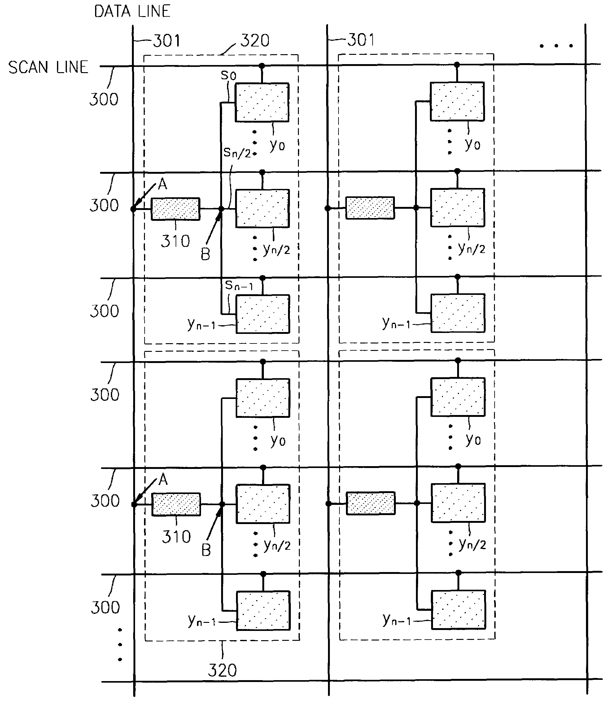
[0020]An active matrix organic light emitting diode (OLED) display panel circuit having a threshold voltage compensation block according to the present invention is shown in FIG. 3, and structural examples of the threshold voltage compensation circuit block of FIG. 3 are shown in FIGS. 4 through 7.

[0021]Referring to FIG. 3, in the active drive OLED display panel circuit structure according to the present invention scan lines 300 and data lines 301 are arranged in rows and columns, respectively. An input terminal A of a threshold voltage compensation circuit block 310 is connected to a data line 301, and ...


PUM


Abstract

An active matrix organic light emitting diode display panel circuit capable of reducing current and brightness nonuniformities between pixels by including a threshold voltage compensation circuit block between a data line and the pixels is provided. The threshold voltage of a video signal loaded in a data line is compensated for while the video signal passes through the threshold voltage compensation circuit block and then provided to a driving transistor of the pixels. One threshold voltage compensation circuit block is connected commonly to a plurality of pixels, rather than be connected to every pixel, so that threshold voltage compensation can be achieved for high-quality, large-sized displays, without increasing the number of transistors for the pixels.

Description

BACKGROUND OF THE INVENTION[0001]This application claims the priority of Korean Patent Application No. 2002-55995, filed Sep. 14, 2002, in the Korean Intellectual Property Office, the disclosure of which is incorporated herein in its entirety by reference.[0002]1. Field of the Invention[0003]The present invention relates to a panel circuit structure for an active matrix organic light emitting diode display, capable of reducing current nonuniformities between pixels and nonuniformity in the brightness of the display.[0004]2. Description of the Related Art[0005]Conventionally, an active matrix organic light emitting diode panel circuit structure, as shown in FIG. 1, is widely known, where a plurality of pixels, each of which includes two thin film transistors, a capacitor, and an organic light emitting diode (OLED), are arranged in rows and columns.[0006]As is well known, in the conventional active matrix OLED panel circuit, upon selection of a scan line 100 a video signal loaded in a...

Claims


Application Information

Patent Timeline
Patent Type & Authority Patents(United States)
IPC IPC(8): G09G3/32G09G3/30
CPCG09G3/3233G09G2300/0465G09G2300/0819G09G2300/0842G09G2320/0233G09G2320/043G09G3/30
Inventor CHUNG, CHOONG-HEUIHWANG, CHI-SUNSONG, YOON-HOLEE, JIN-HO
Owner UNILOC 2017 LLC
Why Eureka
Try Eureka