Mold type semiconductor laser

a semiconductor laser and mold-type technology, applied in semiconductor lasers, optical beam sources, instruments, etc., can solve the problem that the laser output cannot be fixed, and achieve the effect of accurate optical output control circuits

Inactive Publication Date: 2005-11-29
ROHM CO LTD
View PDF17 Cites 6 Cited by
  • Summary
  • Abstract
  • Description
  • Claims
  • Application Information

AI Technical Summary

Benefits of technology

[0005]It is an object of the present invention to solve the above-stated problem and to provide a mold type semiconductor laser capable of forming an accurate optical output control circuit by constantly detecting accurate laser output and operable with constantly fixed output.

Problems solved by technology

Due to this, it was discovered that even if the output of the laser chip actually has no change, the output detected by the light receiving element varies with temperature and that if the laser output is controlled based on the varying output, the laser output cannot be made fixed.

Method used


Image

  • Mold type semiconductor laser
  • Mold type semiconductor laser
  • Mold type semiconductor laser

Examples


Embodiment Construction

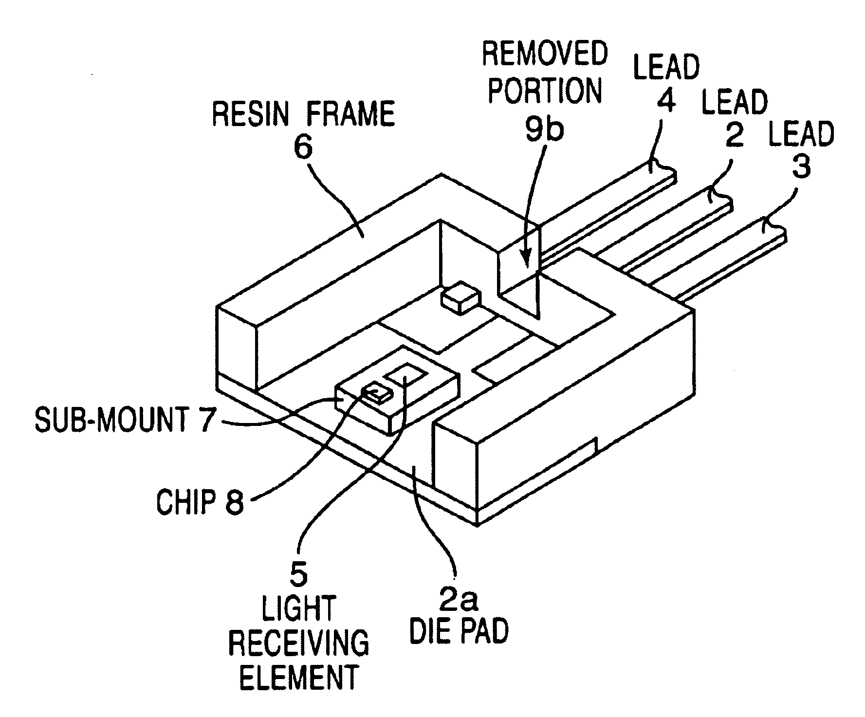
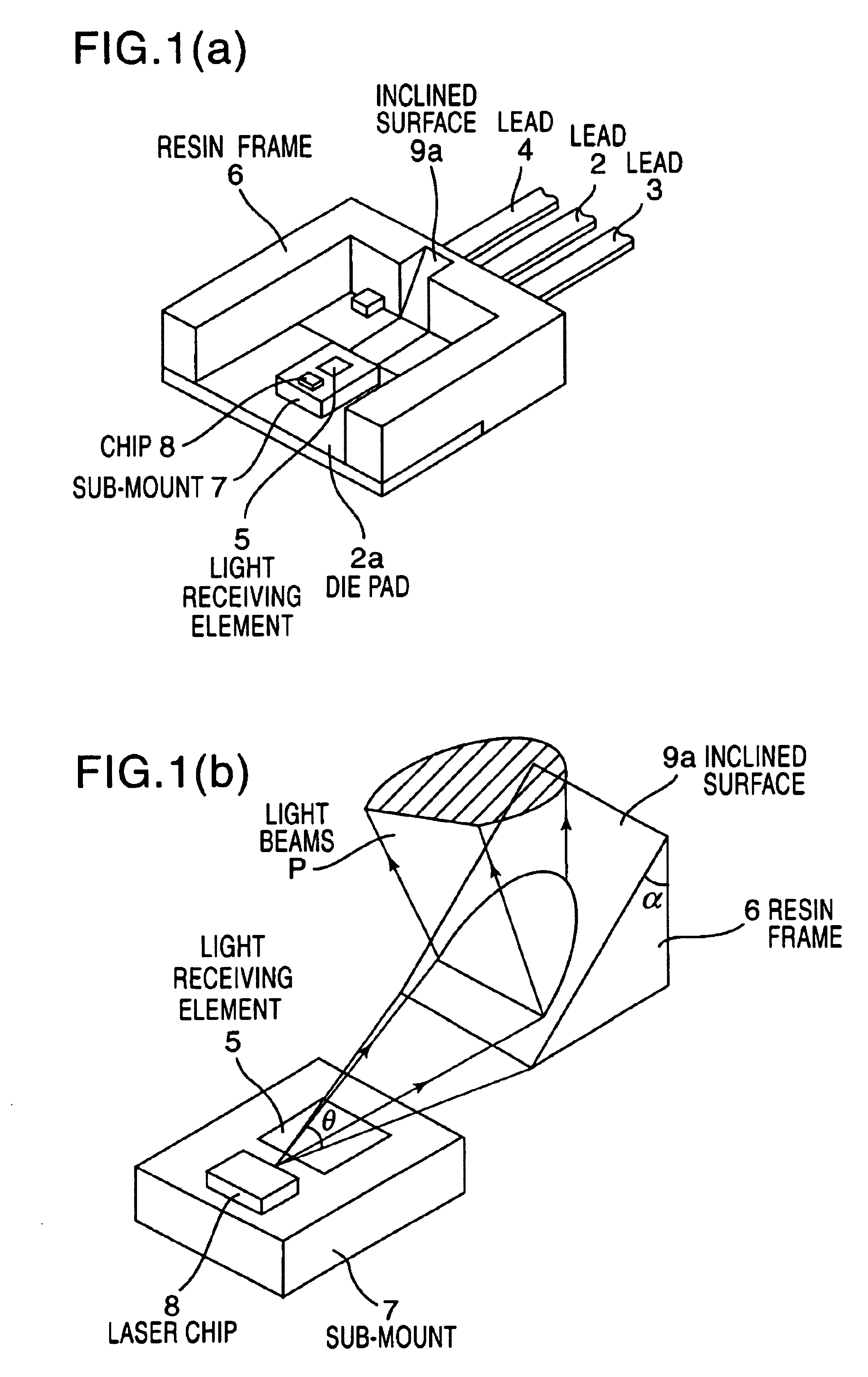
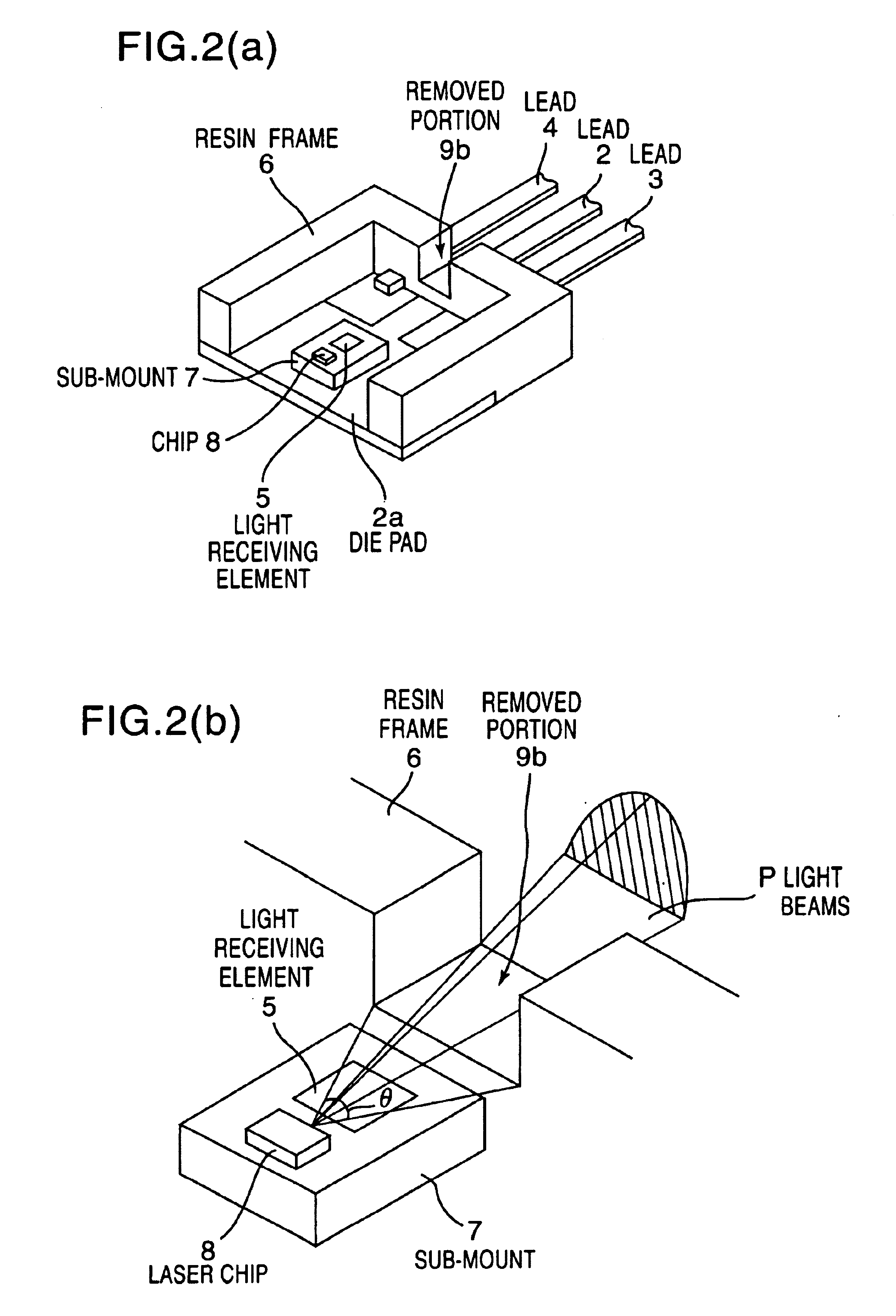
[0017]A mold type semiconductor laser according to the present invention has a sub-mount 7 which is mounted on a die pad portion 2a of the first lead (or a common lead) 2 having the die pad portion 2a formed on one end portion thereof, and on which a laser chip 8 and a monitoring light receiving element 5 are provided, as shown in FIGS. 1(a) and 1(b) which are explanatory views for one embodiment thereof. The electrode of the laser chip 8 and the electrode of the light receiving element 5 are electrically connected to the second leads 3 and 4 by wires such as metallic wires, not shown, respectively. A resin frame 6 is provided to cover the sides and a rear end side of the sub-mount 7 except for the emission surface side of the laser chip 8 and to integrally hold one end portion sides of the first and second leads 2, 3 and 4. An antireflection means 9 (9a) for preventing light from being reflected on the light receiving element 5 is formed on the portion of the resin frame 6 opposite...


PUM

PropertyMeasurementUnit
angleaaaaaaaaaa
angleaaaaaaaaaa
angleaaaaaaaaaa

Abstract

A sub-mount (7) provided with a laser chip (8) and a light receiving element (5) for monitoring is bonded to a die pad portion (2a) of a first lead (2). An electrode of the laser chip and an electrode of the light receiving element are electrically connected to second leads (3, 4) by wires such as metallic wires, not shown, respectively. A resin frame (6) is provided to cover sides and a rear surface side of the sub-mount except for an emission surface side of the laser chip and to integrally hold one end portion sides of the first and second leads. An antireflection unit (9) for preventing light from being reflected on the light receiving element is formed on a portion of the resin frame opposite to the rear end face of the laser chip. As a result, it is possible to obtain a mold type semiconductor laser capable of constantly detect accurate laser chip output and capable of forming an accurate optical output control circuit.

Description

FIELD OF THE INVENTION[0001]The present invention relates to a semiconductor laser particularly suited to be used as a pickup light source for a CD (compact disk), a DVD (digital versatile disk), an LBP (laser beam printer), a DVD-ROM or the like. More specifically, the present invention relates to a mold type semiconductor laser having a structure in which the influence of light reflection due to a resin-molded frame is eliminated while a laser chip is die-bonded to a lead frame and the resin-molded frame protects the periphery of the lead frame.BACKGROUND OF THE INVENTION[0002]A mold type semiconductor laser is disclosed by, for example, Japanese Patent No. 2951077 and constituted as shown in FIG. 5. In FIG. 5, a sub-mount 7 on which a laser (or LD) chip 8 is bonded is mounted on the die pad portion 2a on the tip end of a common lead 2 among three leads 2, 3 and 4 formed integrally as a lead frame 1. The LD chip 8 and a light receiving element 5 for monitoring are wire-bonded to t...

Claims


Application Information

Patent Timeline
Patent Type & Authority Patents(United States)
IPC IPC(8): G11B7/13G11B7/125G11B7/135H01L31/12H01S5/00H01S5/0232H01S5/042
CPCH01S5/02248H01S5/02244H01S5/0683H01S5/0231H01S5/02325H01S5/0232H01S5/30
Inventor NAKATA, NAOTARO
Owner ROHM CO LTD
Why Eureka
Try Eureka