Input/output structure and integrated circuit using the same

a technology of input/output structure and integrated circuit, which is applied in the direction of semiconductor devices, semiconductor/solid-state device details, electrical devices, etc., can solve the problems of complicated serial link technology, version control, logistics control and circuit design, and inconvenient integration of these two standards, so as to simplify the design and reduce the cost

Active Publication Date: 2005-12-06
VIA TECH INC
View PDF2 Cites 4 Cited by
  • Summary
  • Abstract
  • Description
  • Claims
  • Application Information

AI Technical Summary

Benefits of technology

[0010]An object of the present invention is to provide an I / O structure and IC using the same to support several standards such as PCIE and AGP interface standards. The IC having the I / O structure shares the same conducting wires, the same bonding pads, and the same substrate so that the device applying the IC can use the same buses and the same motherboard to reduce the costs and simplify the design. In addition, the number of the die pads can be saved for the die pads for power source and ground purpose.
[0014]The I / O structure of the present invention connects the PCIE I / O pad and the AGP I / O pad to the same die pad. Hence, the IC using the I / O structure can support several standards, and both standards can share the same conducting wire, the same bonding pad and the same substrate. The device using the IC only uses the same bus layout and the same motherboard to support several standards. In addition, the number of the die pads can be reduced for other uses such as power pads and ground pads.

Problems solved by technology

Hence, it causes the inconvenience of the version control, logistics control and the circuit designs.
PCIE interface standard uses current source to drive and a very complex serial link technology.
Hence, it is very difficult to integrate these two standards and use the same I / O pad to support PCIE interface standard and the AGP interface standard.
Hence, the layout and the circuit design would be very complicated, which causes the design and manufacturing of the motherboards too complicated.

Method used


Image

  • Input/output structure and integrated circuit using the same
  • Input/output structure and integrated circuit using the same

Examples


Embodiment Construction

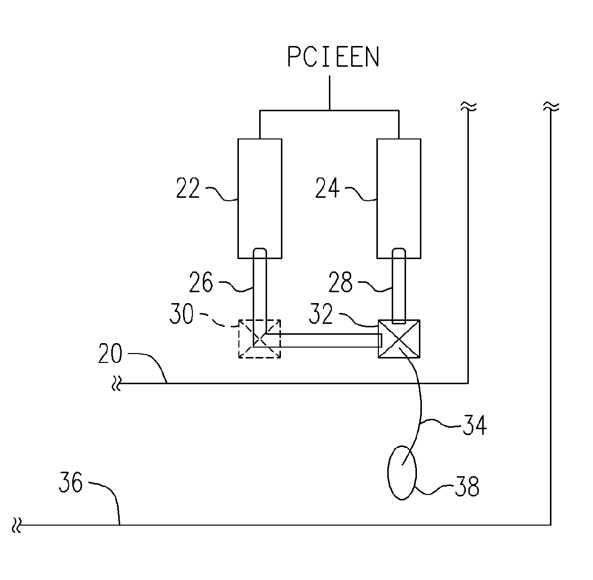
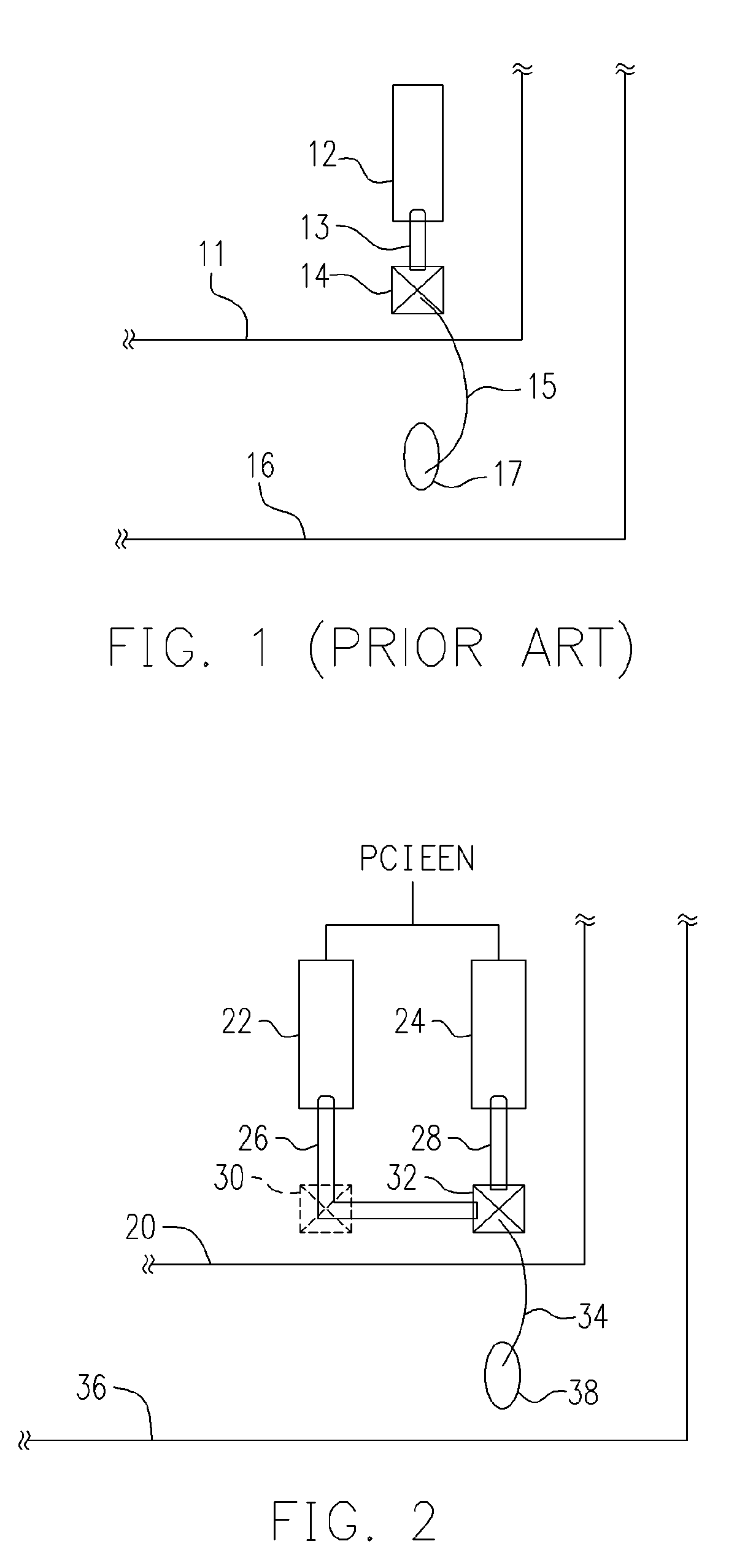
[0018]FIG. 2 is an I / O structure supporting a plurality of interface standards in accordance with a preferred embodiment of the present invention. In this embodiment, we use the PCIE and AGP standards as examples. It is well known that PCIE standard and the AGP standard have different transmitting / receiving structures. PCIE standard uses current source to drive and a very complex serial link technology. The AGP standard uses the conventional I / O such as open-drained (AGP 3.0) or push-pull (AGP 2.0) structure. Hence, it is very difficult to integrate these two standards and use the same I / O pad to support PCIE standard and the AGP standard. Therefore, the present invention does not integrate both standards into the same I / O pad. The present invention keeps the PCIE I / O pad and the AGP I / O pad intact so that the driving ability and the ESD protection of the I / O pads will not be affected.

[0019]Referring to FIG. 2, the I / O structure for the die 20 can support two standards such as PCIE ...


PUM


Abstract

An input / output structure for a die to support an Accelerated Graphic Port (AGP) standard and a Peripheral Component Interconnection Express (PCIE) standard is provided. The I / O structureis suitable for the die pad. It comprises: a PCIE input / output pad for supporting PCIE standard; an AGP input / output pad for supporting AGP standard; a die pad coupled to an external circuit; a first conducting distributed wire coupled to the PCIE input / output pad and the die pad; and a second conducting distributed wire coupled to the AGP input / output pad and the die pad; wherein only one of the PCIE input / output pad and the AGP input / output pad is enabled at the same time.

Description

CROSS REFERENCE TO RELATED APPLICATIONS[0001]This application claims the priority benefit of Taiwan application serial no. 92127763, filed Oct. 7, 2003.BACKGROUND OF INVENTION[0002]1. Field of the Invention[0003]This invention generally relates to an I / O structure in the integrated circuit, and more particularly to an I / O structure for a die using the same die pad to support several interface standards.[0004]2. Description of Related Art[0005]To effectively protect the die from being damaged and to make the die be connected to the external circuit, the packaging technology has been widely used. There are several technologies for chip packaging. For chip bonding technology, wire bonding, flip chip, and tape automatic bonding are the most common bonding technologies, wherein the wire bonding technology is the maturest among these bonding technologies.[0006]For the wire bonding technology, there are several I / O pads on the die. Those I / O pads are coupled to the die pads on the active s...

Claims


Application Information

Patent Timeline
Patent Type & Authority Patents(United States)
IPC IPC(8): H01L23/50H01L23/525
CPCH01L23/50H01L23/525H01L2224/48091H01L2224/48227H01L2924/00014H01L24/48H01L2224/05554H01L2924/14H01L2924/00H01L2224/45099H01L2224/45015H01L2924/207
Inventor CHANG, CHI
Owner VIA TECH INC
Why Eureka
Try Eureka