Plasma processing system control

a technology of processing system and control panel, which is applied in the direction coating, electric discharge lamp, etc., can solve the problems of high equipment cost, relatively large volume of plasma processing environment, and the need for complex and expensive electrical isolation techniques for ion-energy analyzer collectors in the vicinity of highly energized electrodes

Active Publication Date: 2005-12-06
LAM RES CORP
View PDF3 Cites 65 Cited by
  • Summary
  • Abstract
  • Description
  • Claims
  • Application Information

AI Technical Summary

Benefits of technology

[0010]In yet another embodiment, the invention relates to an arrangement for approximating an ion energy distribution function (IEDF) at a substrate surface of a substrate, the substrate being processed in a plasma processing chamber. There is included a first circuit for obtaining a first voltage value, the first voltage value representing a value of a first voltage that represents a DC potential (VDC) at the substrate surface. There is also included a second circuit for obtaining a peak low frequency RF voltage value (VLFRF(PEAK)) during plasma processing, the peak low frequency RF voltage (VLFRF(PEAK)) value representing a peak value of a low frequency RF voltage (VLFRF) supplied to the plasma processing chamber. Additionally, there is included a computing device configured to compute the IEDF from the first voltage value and the peak low frequency RF voltage (VLFRF(PEAK)) in accordance with f⁡(E)≡(ⅆVLFⅆt)-1,

Problems solved by technology

However, an ion-energy analyzer is an expensive piece of equipment and is relatively bulky to employ in the plasma processing environment.
Furthermore, the presence of an ion-energy analyzer collector in the vicinity of a highly energized electrode necessitates complex and expensive techniques for electrically isolating the ion-energy analyzer collector from the electrodes.

Method used


Image

  • Plasma processing system control
  • Plasma processing system control
  • Plasma processing system control

Examples


Embodiment Construction

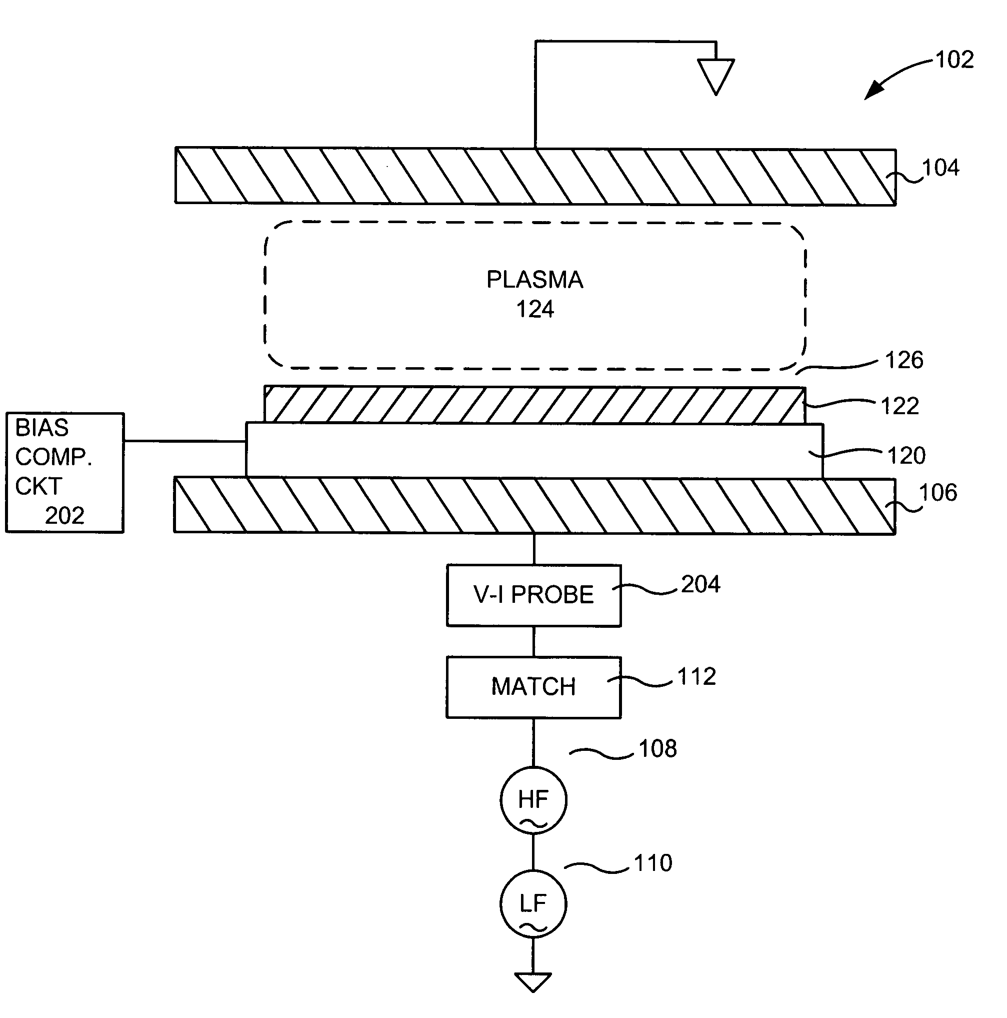
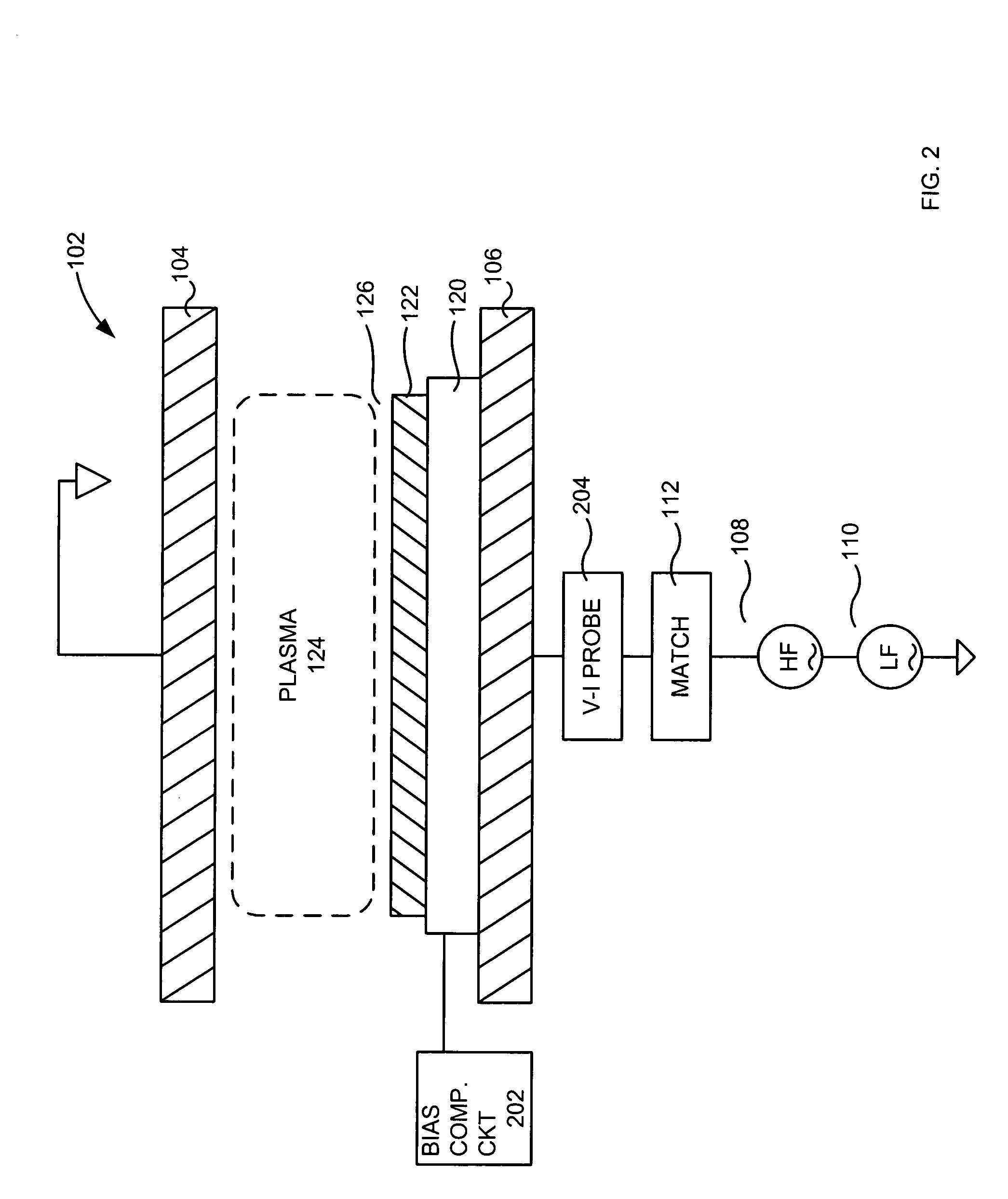
[0018]The present invention will now be described in detail with reference to a few preferred embodiments thereof as illustrated in the accompanying drawings. In the following description, numerous specific details are set forth in order to provide a thorough understanding of the present invention. It will be apparent, however, to one skilled in the art, that the present invention may be practiced without some or all of these specific details. In other instances, well known process steps and / or structures have not been described in detail in order to not unnecessarily obscure the present invention.

[0019]In accordance with one embodiment, there are provided improved methods and apparatus for accurately approximating the ion energy distribution function (IEDF) at the substrate surface using two readily available parameters: the DC potential at the substrate (VDC) and the peak low frequency RF voltage (VLFRF(PEAK)).

[0020]In one embodiment, the bias compensation voltage for the bi-polar...


PUM

PropertyMeasurementUnit
ion energy distribution functionaaaaaaaaaa
frequencyaaaaaaaaaa
bias compensation voltageaaaaaaaaaa

Abstract

A method of approximating an ion energy distribution function (IEDF) at a substrate surface of a substrate, the substrate being processed in a plasma processing chamber. There is included providing a first voltage value, the first voltage value representing a value of a first voltage that represents a DC potential (VDC) at the substrate surface. There is also included providing a peak low frequency RF voltage value (VLFRF(PEAK)) during plasma processing, the peak low frequency RF voltage (VLFRF(PEAK)) value representing a peak value of a low frequency RF voltage (VLFRF) supplied to the plasma processing chamber. There is further included providing a computing device configured to compute the IEDF from the first voltage value and the peak low frequency RF voltage value (VLFRF(PEAK)) in accordance with f(E)(VLFt)-1,
wherein VLF(t)=[(VLFRF(PEAK)-Vdc2)1/2-(VLFRF(PEAK)-Vdc8)1/2sinωt]2.

Description

BACKGROUND OF THE INVENTION[0001]The present invention relates to plasma processing of semiconductor substrates. More particularly, the present invention relates to methods and apparatus for process control during the processing of semiconductor substrates.[0002]In the processing of semiconductor substrates (semiconductor wafers, substrates for Integrated circuit (IC) microelectronics or Micro-electromechanical Systems), it is important to maintain control over the process parameters. Exemplary process parameters include the RF voltage, RF current, the amount of time the process runs, the type and volume of etch and source gas employed, and the like. Over time, it has been found that when a substrate is processed in a plasma processing chamber, ion energy at the substrate surface is an important parameter that may affect many process results such as selectivity, etch rate and / or deposition rate, etch profile, and the like.[0003]To facilitate discussion, FIG. 1 shows an exemplary pla...

Claims


Application Information

Patent Timeline
Patent Type & Authority Patents(United States)
IPC IPC(8): H01J37/32H05H1/00
CPCH01J37/32091H01J37/32935
Inventor MARAKHTANOV, ALEXEI M.HUDSON, ERIC ALLENSADJADI, S. M. REZA
Owner LAM RES CORP
Why Eureka
Try Eureka