RFID (radio frequency identification) and IC card

a technology of radio frequency identification and ic card, which is applied in the field of radio frequency identification and ic cards, can solve the problems of increasing cost, requiring a higher startup receiving power level than an operational receiving power level, and dummy load redesigned, so as to reduce the working voltage margin of the ic, the effect of large variation width of the power supply voltage of the i

Inactive Publication Date: 2005-12-06
RENESAS ELECTRONICS CORP
View PDF10 Cites 107 Cited by
  • Summary
  • Abstract
  • Description
  • Claims
  • Application Information

AI Technical Summary

Benefits of technology

[0007]In a contactless IC card defined in ISO 10536 and ISO 14443, an AC wave received by an antenna coil is rectified and smoothed to provide power source to internal elements of an IC, and communication with an external apparatus is carried out by varying a load on the IC. Thus, a variation width of a power supply voltage of the IC is rather large. Therefore, the power supply voltage is monitored at all times to check whether or not it is within a working guarantee range of the IC. If the power supply voltage is within the working guarantee range, a reset state imposed on the IC is released to operate internal circuits thereof. In this scheme, a hysteresis circuit configuration of a two-stage type is provided in which a reset voltage is given at a working guarantee voltage level and the sum of the reset voltage and a voltage drop due to dynamic load variation is used as a reset release voltage. This condition is a cause of reducing a working voltage margin of the IC.

Problems solved by technology

Hei 8-30752 is disadvantageous in that there is difficulty in application to RFID in which dynamic impedance variation by such means as intermittent load operation is used for communication from an IC card to an external apparatus (this kind of technique is defined in ISO 10536 and ISO 14443).
Although it is possible to apply this circuit arrangement to RFID by superimposing a communication load on the dummy load, there arises a problem that the dummy load must be redesigned according to design changes in load for communication and design changes in antenna coil.
Further, the dummy load must be set to have a value inclusive of upper limits of individual CPU difference, individual communication load difference, and impedance variation with temperature, resulting in a problem that a startup receiving power level higher than an operational receiving power level is required.
Moreover, the complexity of this circuit arrangement gives rise to a problem of an increase in cost.
Hei 10-207580 must be set to have a value corresponding to the sum of a working guarantee voltage and a drop-down voltage inclusive of an upper limit of individual communication load difference (inclusive of impedance variation with temperature) resulting in a problem that a margin of a startup voltage is narrowed.
Still further, there arises a problem of an increase in circuit complexity.
This condition is a cause of reducing a working voltage margin of the IC.
As described above, in conventional contactless IC cards and RFIDs, the settings of a dummy load and a reset release voltage involve external factors, causing a disadvantage of the lack of general versatility and a difficulty in ensuring a maximum of a working voltage range.

Method used


Image

  • RFID (radio frequency identification) and IC card
  • RFID (radio frequency identification) and IC card
  • RFID (radio frequency identification) and IC card

Examples


embodiment 1

[0022]A configuration and circuit operations of a contactless IC card as a form of RFID will first be described below.

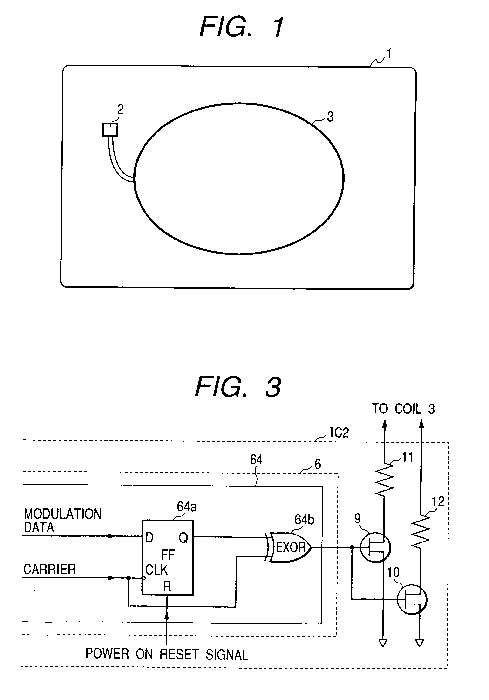
[0023]FIG. 1 presents a general configuration of the contactless IC card. In this figure, there is shown a plan view of a part mounting arrangement on a card base material with a surface layer removed. An IC chip 2 is connected with an antenna coil 3 on an IC card 1.

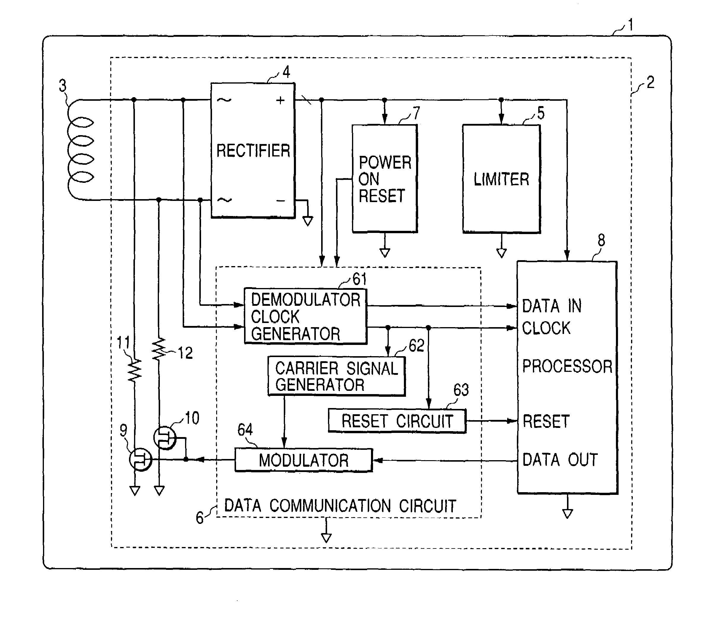
[0024]FIG. 2 presents a general configuration of circuit blocks of the contactless IC card. The circuit block configuration shown in this figure is applicable to implementation of the present invention. Note, however, that an internal structure of a power-on-reset circuit 7 in the present invention is different from those in conventional techniques.

[0025]Referring to FIG. 2, power is received from an external apparatus through the antenna coil 3 contained in the IC card 1. For information interchange with the external apparatus, contactless coupling operations are performed as described below.

[0026]An AC ...

embodiment 2

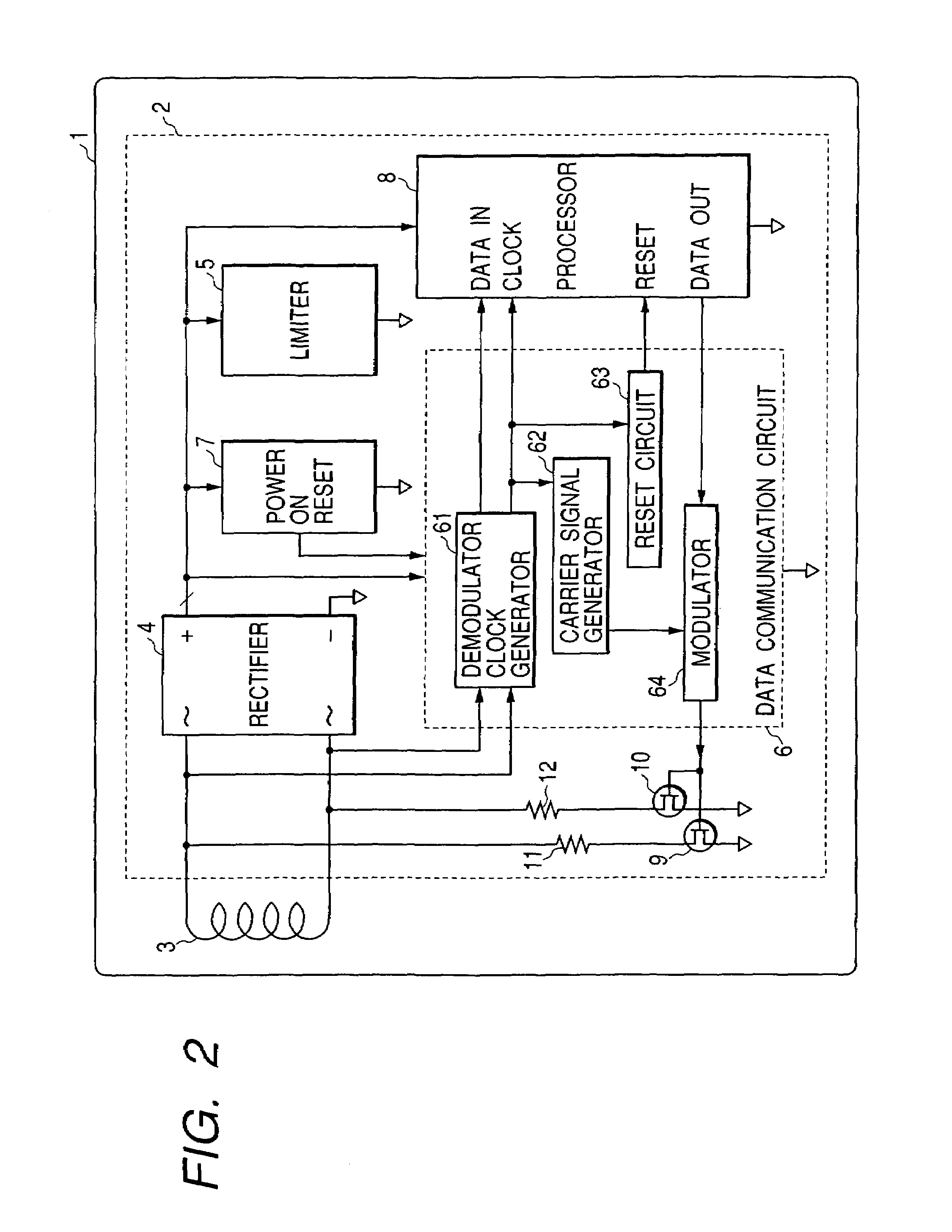
[0046]Referring to FIG. 9, there is shown a partial circuit structure in an IC according to another preferred embodiment of the present invention.

[0047]In FIG. 9, the FETs 9 and 10 and the resistors 11 and 12 perform operations as described in the foregoing (explained in description in connection with FIGS. 3 and 7). An OR circuit 64d is provided between an output terminal of the modulator 64 in the data communication circuit 6 of the IC 2 as a switch operation signal source and the gate terminals of the FETs 9 and 10. As another input to the OR circuit 64d, a power-on-reset signal is applied from the power-on-reset circuit 7. There is provided a circuit arrangement in which an output of the OR circuit 64d has a high level when the power-on-reset signal is high regardless of an output level of the modulator 64. Thus, at the time of resetting, the resistors 11 and 12 are grounded to decrease impedance in the IC 2. That is to say, it is not required to provide a hysteresis characteris...


PUM


Abstract

An RFID which provides a wide working voltage range and general versatility at low cost, without the need for changing its internal circuit design due to external factors. In the RFID, there is provided an arrangement that a low impedance state is given when its internal data communication circuit is in a reset state.

Description

BACKGROUND OF THE INVENTION[0001]The present invention relates to a radio frequency identification (RFID) and an IC card for the RFID, and more particularly to an RFID and a contactless IC card containing the same for receiving power and information from an external apparatus and for transmitting information to the external apparatus on a contactless basis.[0002]An RFID is used as a tag, for example, and an IC card is a kind of the RFID.[0003]In a conventional RFID such as contactless IC card and the like in which power is received from an external apparatus and signals are interchanged with the external apparatus on a contactless basis, an AC wave received by an antenna coil is rectified and smoothed and then supplied to internal circuits through a series regulator. Recently, however, for the purpose of widening a working voltage margin, there has also been used a method of supplying power only by providing a limiter circuit for high voltage resistant protection after rectification...

Claims


Application Information

Patent Timeline
Patent Type & Authority Patents(United States)
IPC IPC(8): B42D15/10G06F1/24G06K19/07H04B7/00H04Q5/22
CPCG06K19/0723G06K19/07
Inventor OHKAWA, TAKEHIROYUYAMA, MIKIYOSHIGI, HIROSHIOONISHI, TADASHIWATANABE, KAZUKI
Owner RENESAS ELECTRONICS CORP
Why Eureka
Try Eureka