CMOS isolation cell for embedded memory in power failure environments

a technology of isolation cell and embedded memory, which is applied in the field of semiconductor memory within an integrated circuit, can solve the problems of increasing the overall solution cost, and the metal oxide semiconductor (cmos) technology used by redundant array of independent disk input/output (io) controllers is not amenable to these techniques, and achieves the effect of preventing data transfer

Inactive Publication Date: 2005-12-20
AVAGO TECH WIRELESS IP SINGAPORE PTE
View PDF4 Cites 13 Cited by
  • Summary
  • Abstract
  • Description
  • Claims
  • Application Information

AI Technical Summary

Benefits of technology

[0006]In an embodiment of the present invention, isolation cells prevent the passage of data signals to and / or from an embedded memory on an integrated circuit chip. The embedded memory and isolation circuitry are preferably exclusively located in a dedicated portion of the wafer. The isolation cells are controlled by one or more enable signals and one or more switches tied to power levels elsewhere present within the integrated circuit. For example, the power for core logic circuitry may control one of the switches. If any power level falls below a threshold level, the switch is turned off, thereby preventing data transfer. The isolation cells of the present invention primarily include one or more series of transistors that are controlled by the enable signals and / or the power levels. Each series of transistors links adjacent transistors by source to drain or drain to drain connections. A series may be formed of transistors in parallel in which the drains are connected to a common node and the sources are connected to a negative power supply or ground. There may be a single series of transistors in a totem pole arrangement. In an embodiment, one or more power levels from the integrated circuit control corresponding gates of transistors.

Problems solved by technology

Typically, this has been done using separate, specialized off-chip RAM components, which increases the overall solution cost.
However, the standard complementary metal oxide semiconductor (CMOS) technology used by redundant array of independent disks (RAID) input / output (IO) controllers is not amenable to these techniques.

Method used


Image

  • CMOS isolation cell for embedded memory in power failure environments
  • CMOS isolation cell for embedded memory in power failure environments
  • CMOS isolation cell for embedded memory in power failure environments

Examples


Embodiment Construction

[0018]Reference will now be made in detail to the presently preferred embodiments of the invention, examples of which are illustrated in the accompanying drawings.

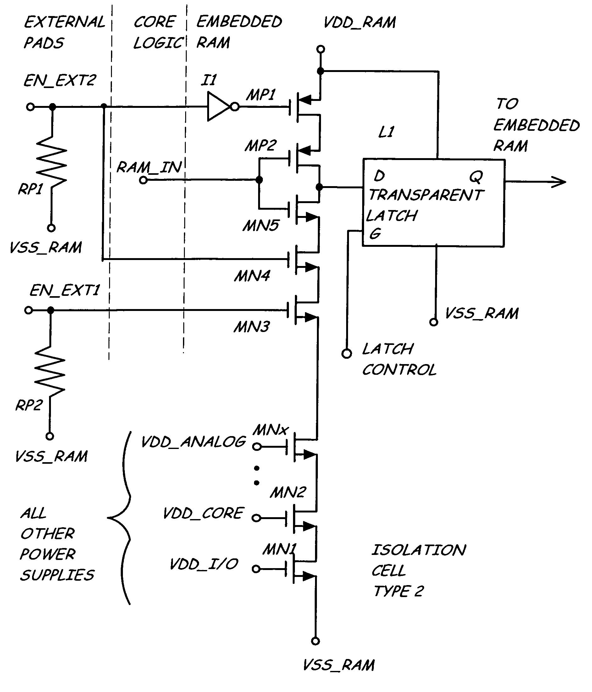
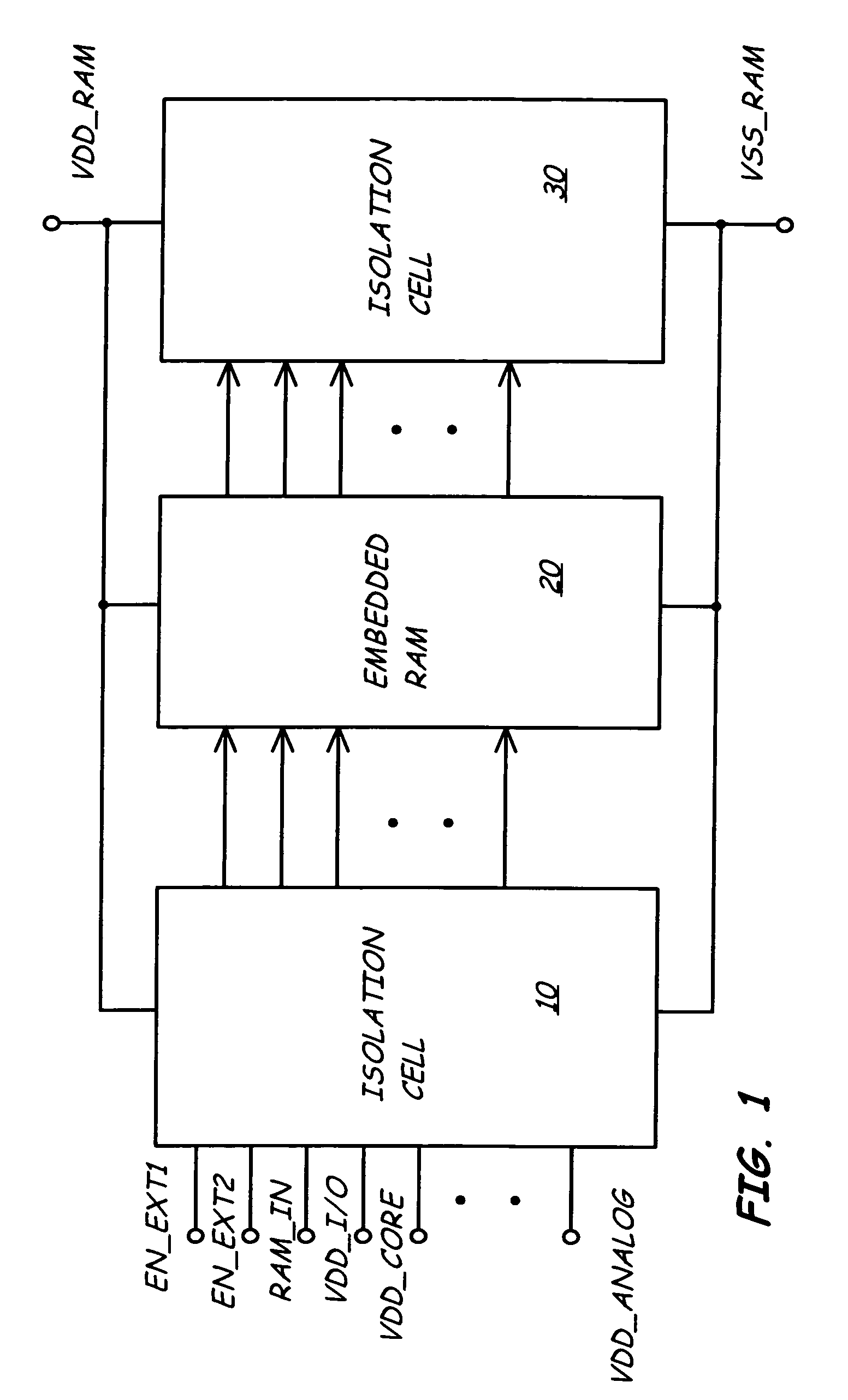
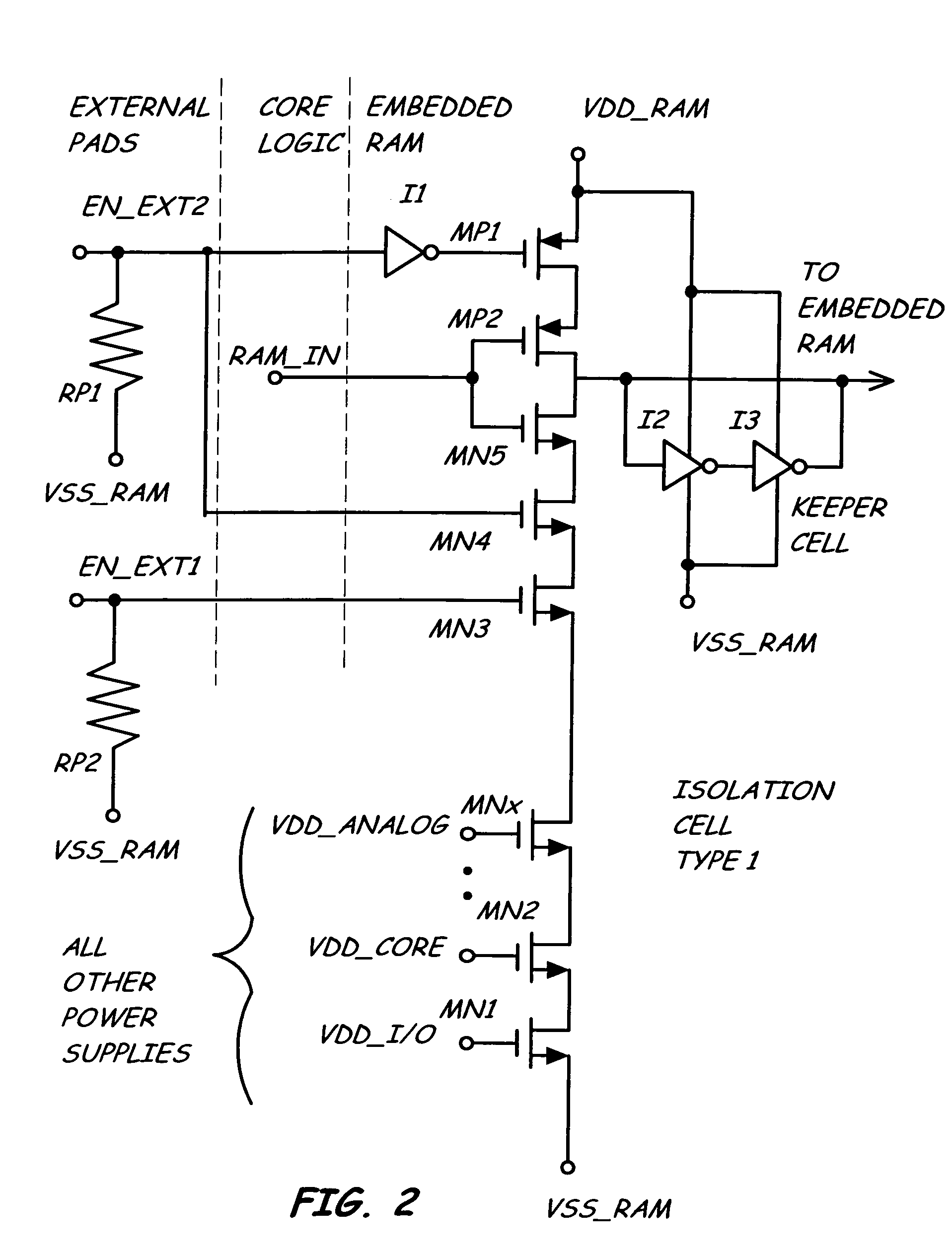
[0019]The present invention relates to an isolation cell useable with an embedded memory on an integrated circuit chip. The isolation cell is preferably controlled by one or more enable signals and tapped power points from integrated circuit circuitry not part of the isolated embedded memory. The present invention also relates to the combination of the isolation cell with the embedded memory. Furthermore, the present invention relates to a method for isolating an embedded memory on an integrated circuit chip. Although the present invention directly relates to the field of RAID IO controllers, it applies to any type of application where data is required to be maintained across power-failure events.

[0020]Electronic systems on a chip contain a variety of functional blocks such as memory, etc. It is often desirable to retain t...


PUM


Abstract

An embedded memory on an integrated circuit chip is capable of being isolated from other on chip and off chip circuitry during power failure modes on the integrated circuit chip. The embedded memory preferably has its own external power supply. When power on chip fails or falls below a threshold level, input to and output from the embedded memory is prohibited by CMOS isolation cells. The CMOS isolation cells are controlled by enable signals and the power level of other power supplies within the integrated circuit.

Description

FIELD OF THE INVENTION[0001]The present invention generally relates to the field of semiconductors, and particularly to semiconductor memory within an integrated circuit.BACKGROUND OF THE INVENTION[0002]Redundant Array of Independent Disks (RAID) controller chips use memory blocks for various functions such as data transfer and storage. RAID controllers require some type of non-volatile storage to maintain information such a data cache in the event of power failure. As the RAID controller's primary function is to ensure data coherency, it must be able to preserve the history of all relevant input / output (IO) activity to the storage medium. Typically, this has been done using separate, specialized off-chip RAM components, which increases the overall solution cost. Providing this same capability within the RAID controller itself reduces the overall cost. One current technique for retaining data uses the non-volatile features such as a floating gate process (MNOS—Metal-Nitride-Oxide-Se...

Claims


Application Information

Patent Timeline
Patent Type & Authority Patents(United States)
IPC IPC(8): G11C5/14
CPCG11C5/14
Inventor DAY, BRIAN A.GASPARIK, FRANTISEK
Owner AVAGO TECH WIRELESS IP SINGAPORE PTE
Why Eureka
Try Eureka