Nonvolatile semiconductor memory device

Inactive Publication Date: 2005-12-20
LAPIS SEMICON CO LTD
View PDF5 Cites 0 Cited by
  • Summary
  • Abstract
  • Description
  • Claims
  • Application Information

AI Technical Summary

Benefits of technology

[0052]The present invention has been made in view of the foregoing problems. It is an object of the present invention t

Problems solved by technology

However, a problem arises in that the MOS transistors are reduced in drive capacity.
Thus, the reduction in the drive capacity of each of the MOS transistors constituting the transfer gate (CM00) incurs a delay in the operation of the control gate electrode.
Since, however, the transfer gate (CM00) needs a long gate width for the purpose of its high withstanding and is required for each control gate electrode, an increase in layout area cannot be avoided.
Therefore, a delay in reading occurs in the path.
There is, however, a possibility that when a defect with a leak has occurred in th

Method used


Image

  • Nonvolatile semiconductor memory device
  • Nonvolatile semiconductor memory device
  • Nonvolatile semiconductor memory device

Examples


Example

[0063]Preferred embodiments of the present invention will be explained hereinafter in detail with reference to the accompanying drawings.

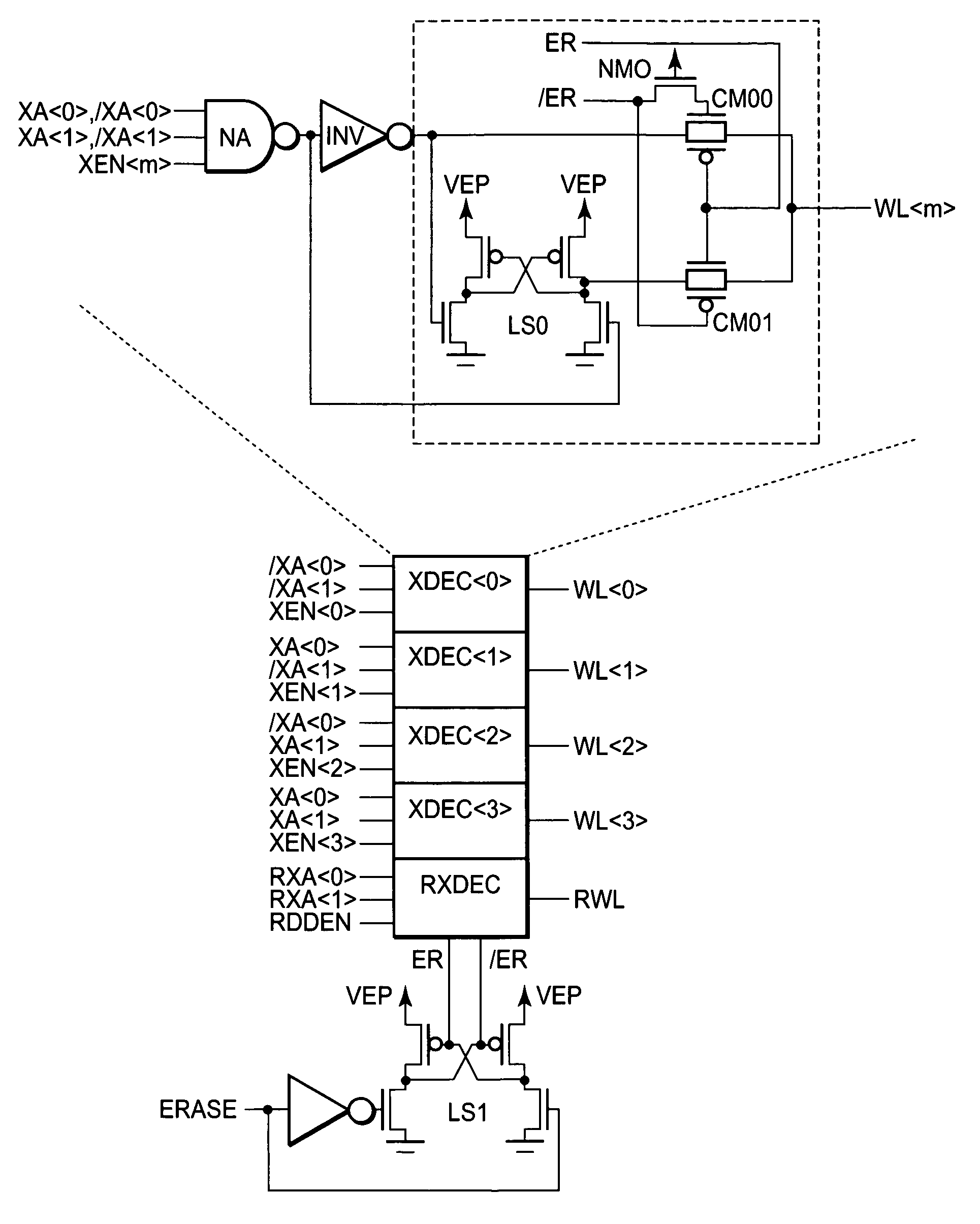
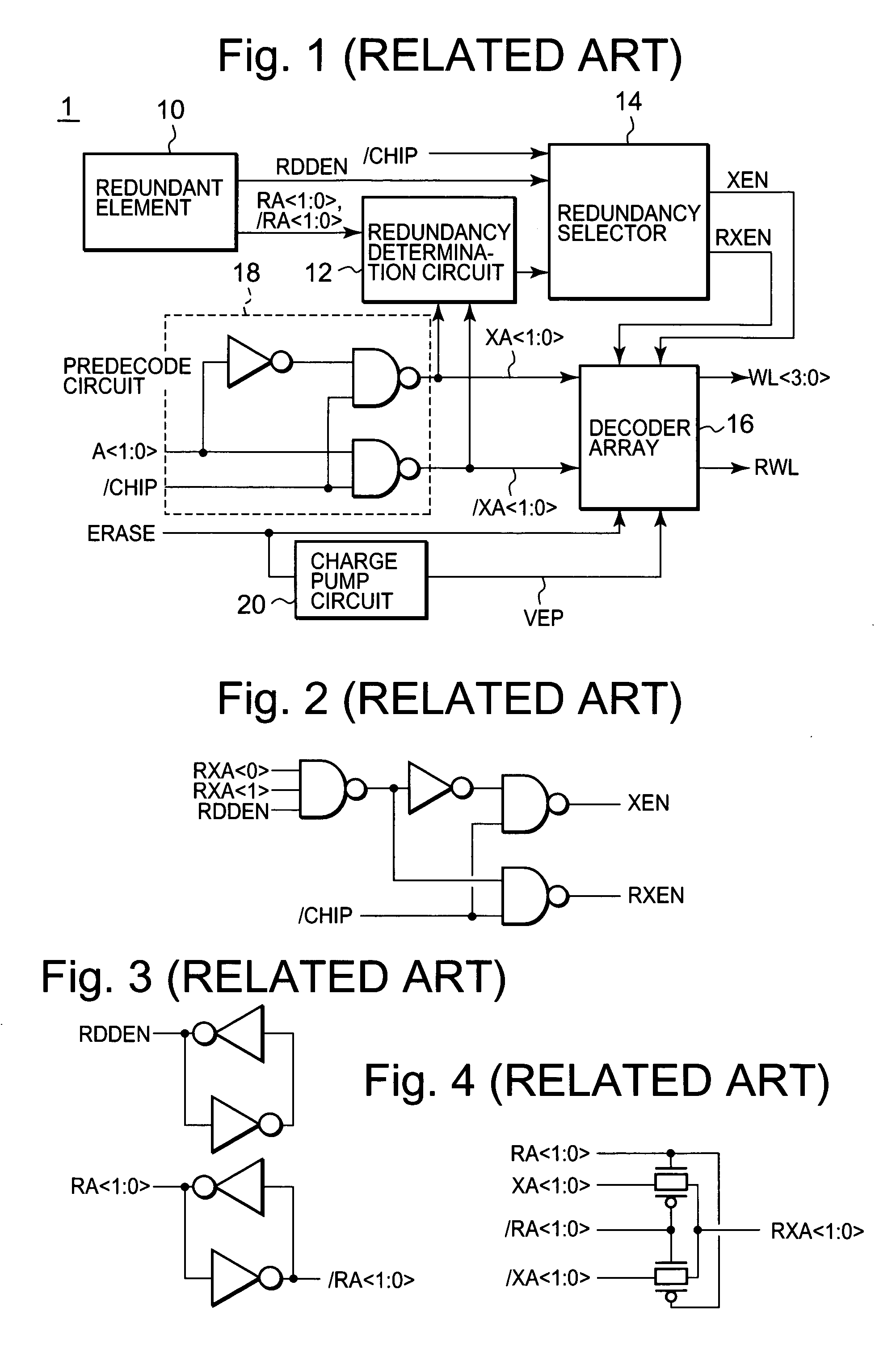
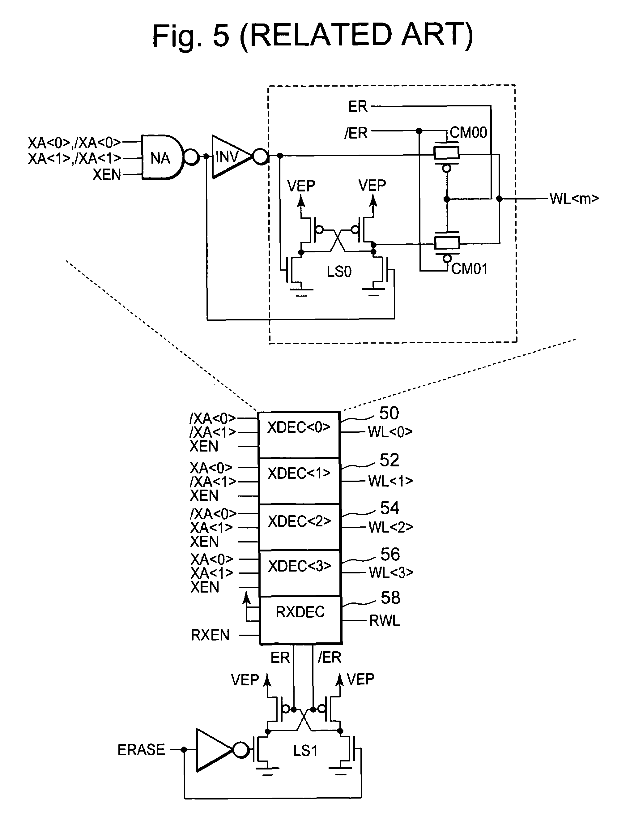
[0064]FIG. 6 is a block diagram showing a configuration of a control gate electrode (WL) type decode circuit of the present invention. FIGS. 7 and 8 are respectively configurational diagrams of respective circuits employed in the present decode circuit. A redundant element and a redundancy determination circuit are similar to the conventional circuits.

[0065]The present decode circuit 60 comprises a predecode circuit 68 which inputs address signals A and a control signal / CHIP, a redundant element 10 which holds and outputs a redundancy replacement flag (RDDEN) and a redundant relief address (RA) set to a power supply level (VCC) where redundancy replacement is required, a redundancy determination circuit 12 which inputs the outputs (RA, / RA) of the redundant element and the outputs (XA, / XA) of the predecode circuit 68, a redundancy selector array ...


PUM


Abstract

The present invention provides a nonvolatile semiconductor memory device capable of achieving the speeding-up of reading and a reduction in layout area. A control gate electrode of each of memory cell transistors employed in the nonvolatile semiconductor memory device according to the present invention is configured so as to be capable of assuming a first power supply potential (VCC) and a second power supply potential (VPP) higher than the first power supply potential upon its operation. A second NMOS transistor is provided between the gate of a first NMOS transistor that drives a control gate electrode (WL) to the first power supply potential (VCC) and a control signal (/ER) connected to the gate thereof. The source of the second NMOS transistor is inputted with the control signal (/ER) and the drain thereof is connected to the gate of the first NMOS transistor. A PMOS transistor is provided in parallel with the first NMOS transistor. A transfer gate comprising these NMOS and PMOS transistors drives the control gate electrode (WL).

Description

BACKGROUND OF THE INVENTION[0001]1. Field of the Invention[0002]The present invention relates to a semiconductor nonvolatile memory, and particularly to a decode circuit suitable for an electrically data reprogrammable flash memory.[0003]2. Description of the Related Art[0004]An EEPROM has been known as an electrically erasable programmable semiconductor nonvolatile memory. A general EEPROM takes a stacked structure in which a memory cell transistor has a floating gate electrode and a control gate electrode. Upon data erasure, a boost or step-up level (VPP: about 12V) higher than a power supply level (VCC) used in a normal circuit is applied to a control gate electrode (WL) to pull or draw out electrical charges from a flowing gate electrode, thereby controlling the amount of the electrical charges in the floating gate electrode. That is, the amount of the electrical charges in the floating gate electrode is reduced to thereby bring the memory cell transistor into conduction when th...

Claims


Application Information

Patent Timeline
IPC IPC(8): G11C8/00G11C29/00
CPCG11C29/82G11C29/84
Inventor MATSUI, KATSUAKI
Owner LAPIS SEMICON CO LTD
Why Eureka
Try Eureka