Semiconductor device

Inactive Publication Date: 2009-07-30
RENESAS ELECTRONICS CORP
View PDF6 Cites 1 Cited by
  • Summary
  • Abstract
  • Description
  • Claims
  • Application Information

AI Technical Summary

Benefits of technology

[0020]According to the semiconductor device of the present invention, it is po

Problems solved by technology

However, this method causes a problem as follows.
As such, although the number of pads can be reduce

Method used


Image

  • Semiconductor device
  • Semiconductor device
  • Semiconductor device

Examples


Example

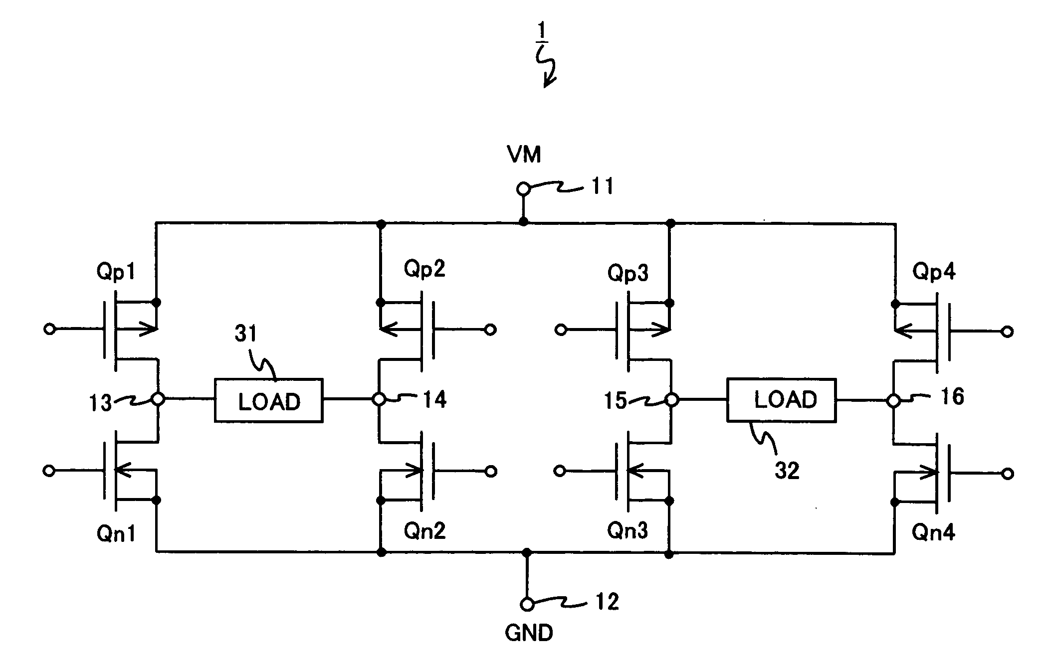
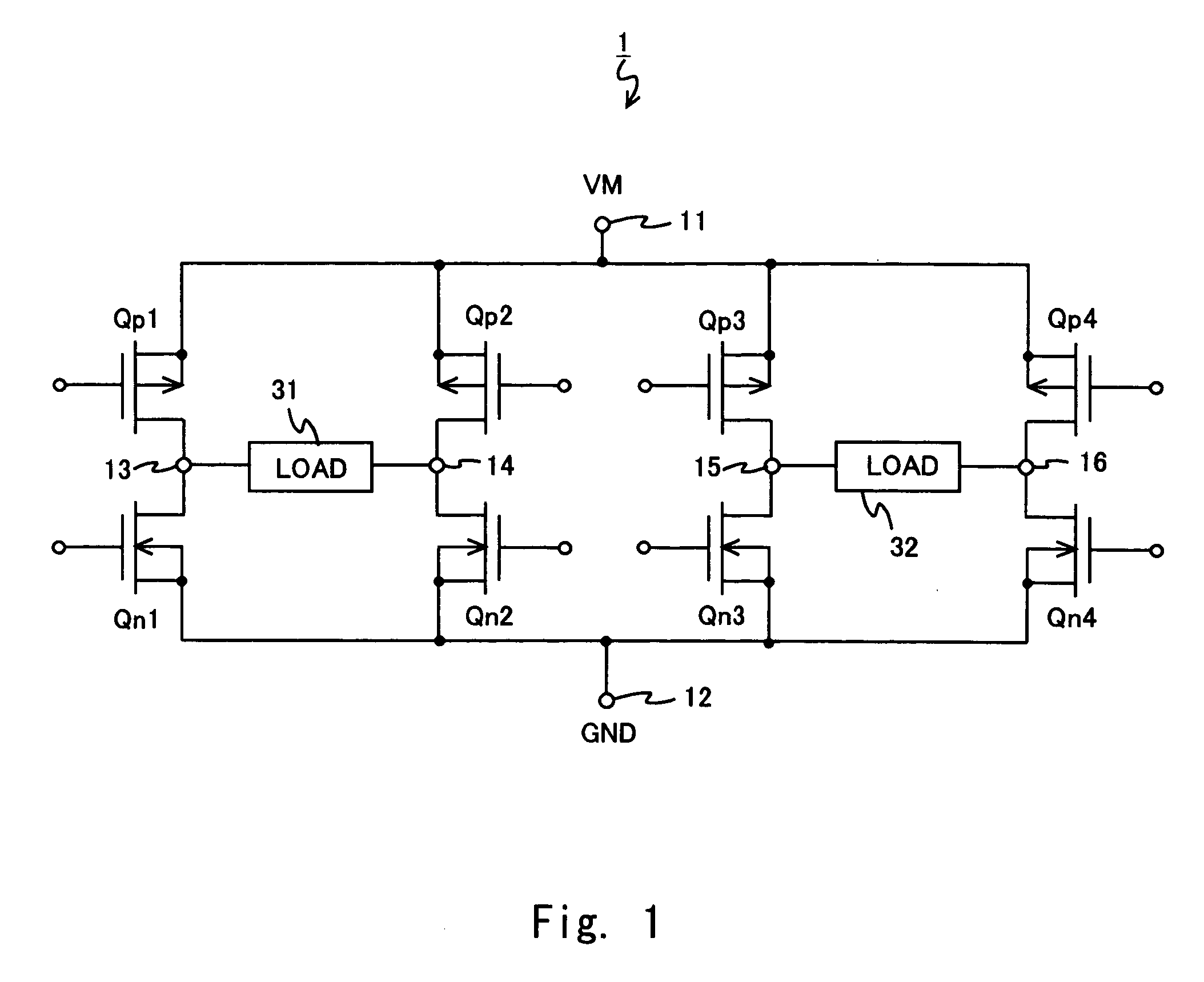
[0037]The components used in [WHAT IS CLAIMED IS] are added with parentheses to the numbers or symbols used in [DETAILED DESCRIPTION OF THE EXEMPLARY EMBODIMENTS] below in order to make clear the correspondence relation between the numbers or symbols used in [DETAILED DESCRIPTION OF THE EXEMPLARY EMBODIMENTS] and the components used in [WHAT IS CLAIMED IS]. However, it is not intended to use the correspondence relation for interpreting the technical scope of the invention described in [WHAT IS CLAIMED IS]. Now, an exemplary embodiment of the present invention will be described with reference to the drawings. FIG. 1 shows an H bridge circuit 1 with a two-channel structure according to the exemplary embodiment of the present invention. The H bridge circuit 1 includes P type power MOS transistors Qp1 (seventh transistor), Qp2 (third transistor), Qp3 (fourth transistor), Qp4 (eighth transistor), N type power MOS transistors Qn1 (fifth transistor), Qn2 (first transistor), Qn3 (second tra...


PUM


Abstract

A semiconductor device includes a first conductive type first transistor, a first conductive type second transistor, a first power supply pad arranged between the first transistor and the second transistor and supplying a first potential, a second conductive type third transistor, a second conductive type fourth transistor, a second power supply pad arranged between the third transistor and the fourth transistor and supplying a second potential, a first output pad arranged between the first transistor and the third transistor, and a second output pad arranged between the second transistor and the fourth transistor, in which a direction in which a line connecting the first power supply pad with the second power supply pad extends is perpendicular to a direction in which a line connecting the first output pad with the second output pad extends.

Description

BACKGROUND[0001]1. Field of the Invention[0002]The present invention relates to a semiconductor device, and more particularly, to a semiconductor device including an H bridge circuit.[0003]2. Description of Related Art[0004]H bridge circuits formed of power transistors are mainly used for drive control of motors, and in recent years, embedded in semiconductor devices for use.[0005]FIG. 10 shows an H bridge circuit 100 generally having a two-channel structure as a related art. The H bridge circuit 100 includes P type power MOS transistors Qp1, Qp2, Qp3, and Qp4, N type power MOS transistors Qn1, Qn2, Qn3, and Qn4, and loads 131 and 132 such as motors. Each of the P type power MOS transistors Qp1 to Qp4 and each of the N type power MOS transistors Qn1 to Qn4 form a pair, respectively, and each pair is connected in series between VM pads 111 supplying a power supply voltage VM and GND pads 112 supplying a ground voltage GND. The loads 131 and 132 are connected between output pads 113. ...

Claims


Application Information

Patent Timeline
IPC IPC(8): H03K17/56
CPCH01L27/0207H03K17/6872H01L27/092
Inventor ARAKI, NORIHIKO
Owner RENESAS ELECTRONICS CORP
Why Eureka
Try Eureka