Convolutional interleaving and de-interleaving circuit and method thereof

Inactive Publication Date: 2007-03-15
SUNPLUS TECH CO LTD
View PDF7 Cites 13 Cited by
  • Summary
  • Abstract
  • Description
  • Claims
  • Application Information

AI Technical Summary

Benefits of technology

[0012] Accordingly, the present invention is directed to provide a convolutional interleaving and convolutional de-interleaving circuit to decrease the gate count so as to achieve the purpose of reducing the chip layout area.
[0013] The present invention is also directed to provide a convolutional interleaving and convolutional de-interleaving circuit which will save the manufacturing cost.
[0018] In the present invention, an adder is commonly shared and memory addresses are appropriately arranged, the requirement of registers is thus reduced. Accordingly, the required gate count and the chip layout area can be reduced.

Problems solved by technology

During data transmission, noise or some unsatisfactory effects of the channels often causes data errors.
However, the ECC has a limitation for the number of error bits.
When unsatisfactory effects of the channels cause too many errors or continuous error bits, the ECC can not correct the errors.
However, a great number of the shift registers in the integrated circuit will result in a waste of the area.
However, the U.S. Pat. No. 5,537,420 still has to use a lot of adders and high bit registers that unavoidably increases a lot of unnecessary gate counts and limits the chip layout.

Method used


Image

  • Convolutional interleaving and de-interleaving circuit and method thereof
  • Convolutional interleaving and de-interleaving circuit and method thereof
  • Convolutional interleaving and de-interleaving circuit and method thereof

Examples


Embodiment Construction

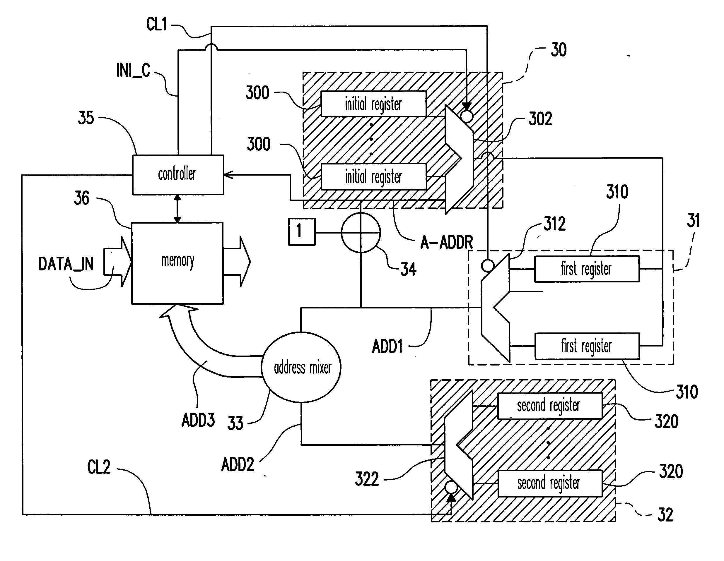
[0028]FIG. 3 is a schematic block diagram of a convolutional interleaving circuit and convolutional de-interleaving circuit according to the embodiment of the present invention. Referring to FIG. 3, the circuit comprises an initial address generator 30, a first address generator 31, a second address generator 32, an address mixer 33, an adder 34, a controller 35 and a memory 36.

[0029] Wherein, the initial address generator 30 includes a plurality of initial registers 300 and an initial selector 302. The first address generator 31 includes a plurality of first registers 310 and a first selector 312. The second address generator 32 includes a plurality of second registers 320 and a second selector 322.

[0030] A plurality of initial registers 300 of the initial address generator 30 store a plurality of initial addresses respectively. The initial selector 302 of the initial address generator 30 receives an initial control signal INI_C from the controller 35 and an accumulating address ...


PUM


Abstract

A convolutional interleaving and de-interleaving circuit and the method thereof are disclosed. The convolutional interleaving and de-interleaving circuit comprises an initial address generator, a first address generator, a second address generator, an address mixer, an adder, a controller and a memory. Wherein, the controller enables those address generators to provide or store corresponding channel addresses. Further, an adder is shared and memory addresses are appropriately arranged so as to reduce the requirement of registers. Accordingly, the required gate count and the chip layout area can be reduced.

Description

CROSS-REFERENCE TO RELATED APPLICATION [0001] This application claims the priority benefit of Taiwan application serial no. 94131427, filed on Sep. 13, 2005. All disclosure of the Taiwan application is incorporated herein by reference. BACKGROUND OF THE INVENTION [0002] 1. Field of Invention [0003] The present invention relates to an interleaving and de-interleaving circuit. More particularly, the present invention relates to a convolutional interleaving and de-interleaving circuit and method applicable for the Digital Video Broadcast (DVB) system. [0004] 2. Description of Related Art [0005] The technology of convolutional interleaving circuit and convolutional de-interleaving circuit is widely used in the fields of telecommunication, as Global System for Mobile communication (GSM), Synchronous Digital Hierarchy (SDH), Digital Video Broadcast-Terrestrial (DVB-T). Such technology is used mainly to prevent the data transmission channel from the interference of noise. [0006] During dat...

Claims


Application Information

Patent Timeline
IPC IPC(8): H03M13/00
CPCH03M13/6502H03M13/2732
Inventor LIN, CHIA-CHUN
Owner SUNPLUS TECH CO LTD
Why Eureka
Try Eureka