Address receiving circuit for a semiconductor apparatus

Active Publication Date: 2008-11-20
SK HYNIX INC
View PDF19 Cites 0 Cited by
  • Summary
  • Abstract
  • Description
  • Claims
  • Application Information

AI Technical Summary

Benefits of technology

[0012]An address receiving circuit for a semiconductor apparatus that can reduce a layout area is described herein

Problems solved by technology

Therefore, a large design layout area is required for the latches.
Even if the address is not input until a successive MRS command is inp

Method used


Image

  • Address receiving circuit for a semiconductor apparatus
  • Address receiving circuit for a semiconductor apparatus
  • Address receiving circuit for a semiconductor apparatus

Examples


Embodiment Construction

.”

BRIEF DESCRIPTION OF THE DRAWINGS

[0016]Features, aspects, and embodiments are described in conjunction with the attached drawings, in which:

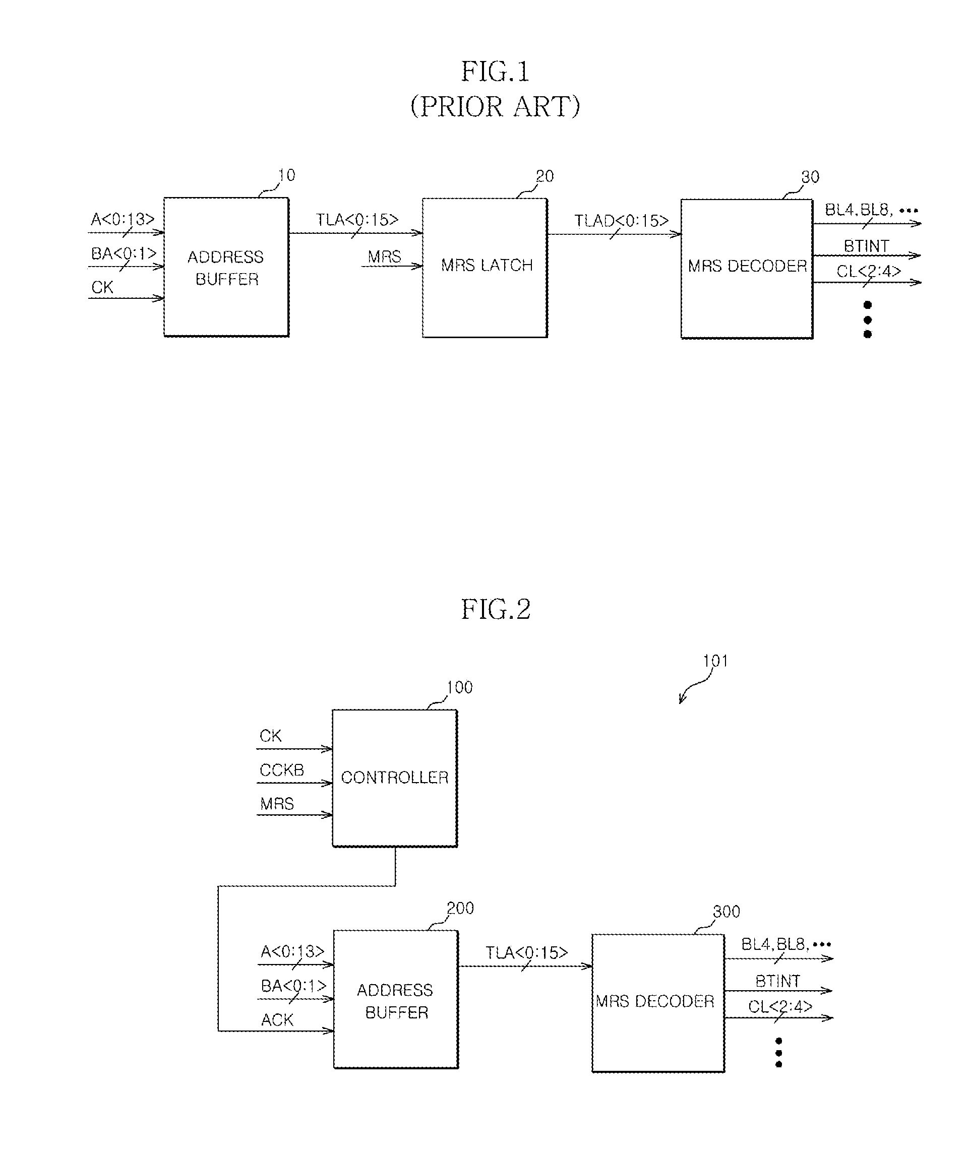
[0017]FIG. 1 is a block diagram showing an exemplary address receiving circuit for a semiconductor apparatus;

[0018]FIG. 2 is a block diagram showing in detail an example address receiving circuit for a semiconductor apparatus according to one embodiment;

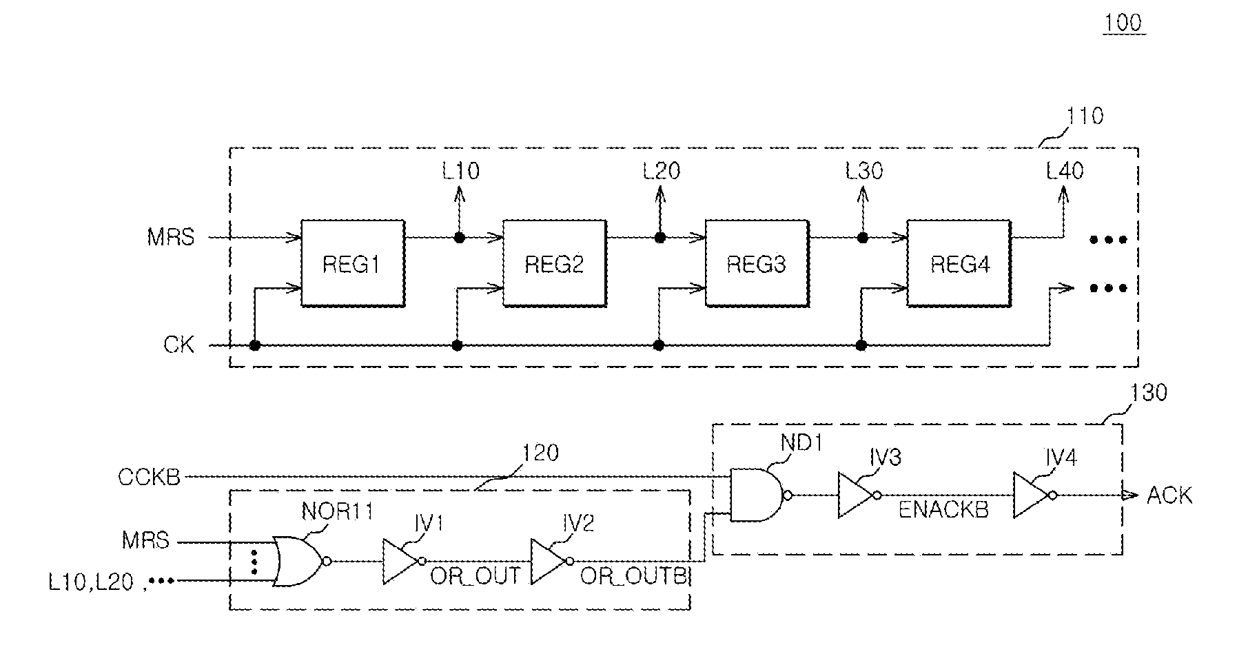
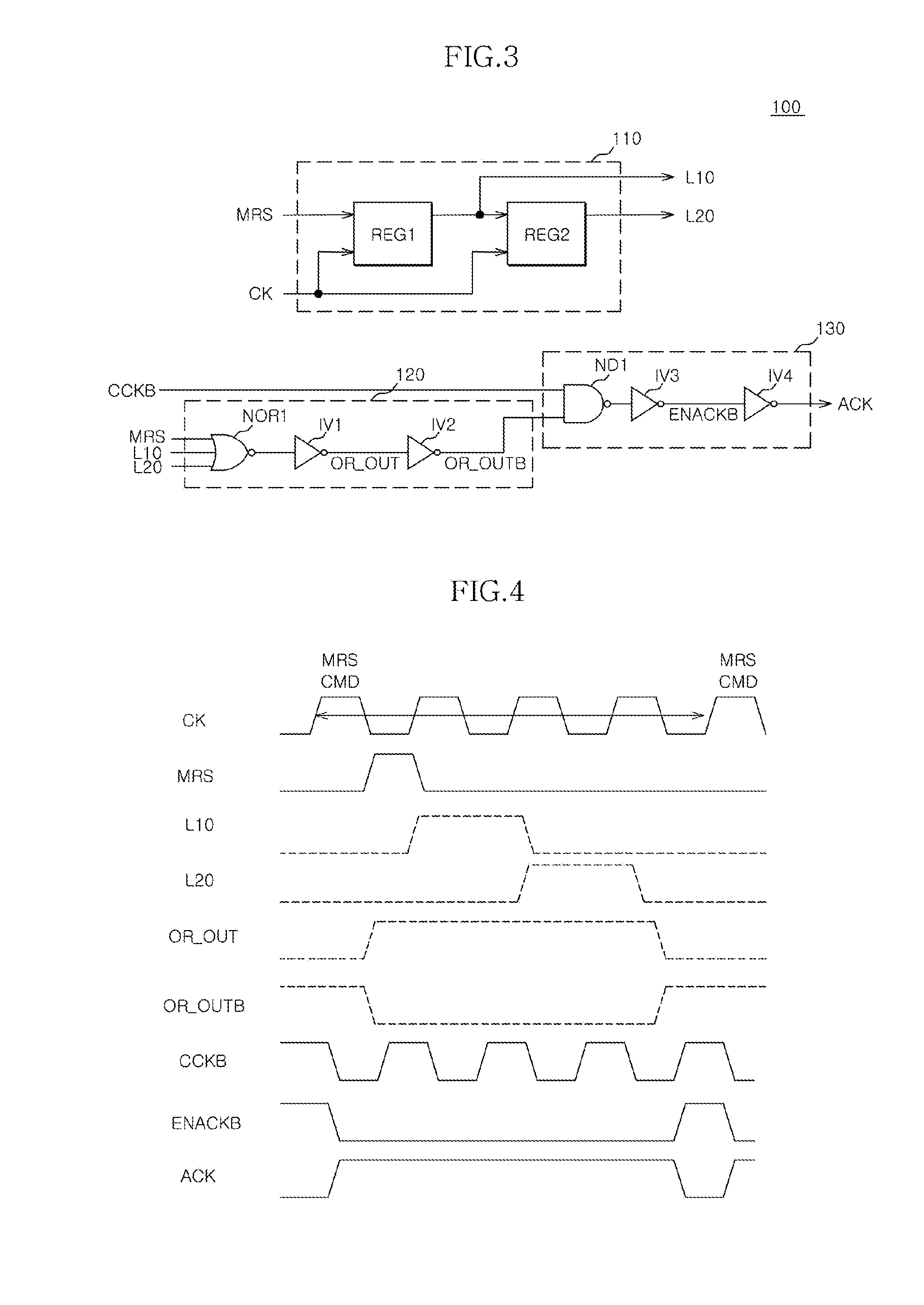
[0019]FIG. 3 is a circuit diagram showing a controller that can be included in the circuit shown in FIG. 2;

[0020]FIG. 4 is a timing diagram illustrating the operation of the address receiving circuit of FIG. 2; and

[0021]FIG. 5 is a circuit diagram showing in detail another example controller that can be included in the circuit shown in FIG. 2.

DETAILED DESCRIPTION

[0022]FIG. 2 is a diagram illustrating an example address receiving circuit 101 configured in accordance with one embodiment. As shown in FIG. 2, the address receiving circuit 101 can include, a controller 100, an address buffer 200, an...


PUM


Abstract

An address receiving circuit for a semiconductor apparatus includes a controller that, in response to a semiconductor apparatus initialization-related command, generates a control signal having an activation cycle corresponding to the standard of cycle time of the semiconductor apparatus initialization-related command, and an address buffer that receives an address according to the control signal.

Description

CROSS-REFERENCE TO RELATED PATENT APPLICATION[0001]The present application claims priority under 35 U.S.C. 119(a) to Korean application number 10-2007-046400, filed on 14 May 2007, in the Korean Patent Office, which is incorporated by reference in its entirety as if set forth in full.BACKGROUND[0002]1. Technical Field[0003]The embodiments described herein relate to a semiconductor apparatus, and in particular, to an address receiving circuit for a semiconductor apparatus.[0004]2. Related Art[0005]As shown in FIG. 1, a conventional receiving circuit includes an address buffer 10, an MRS latch 20, and an MRS decoder 30.[0006]The address buffer 10 receives a general address “A<0:13>” and a bank address “BA<0:1>” according to a clock signal “CK.”[0007]The MRS latch 20 latches an address “TLA<0:15>” output from the address buffer 10 in response to a pulse signal “MRS,” which is generated according to an MRS (Mode Register Set) command. Since the MRS latch 20 must latch ...

Claims


Application Information

Patent Timeline
IPC IPC(8): G11C8/00G11C8/18
CPCG11C8/06G11C8/04G11C8/18
Inventor KIM, KYOUNG-NAMCHO, HO-YOUB
Owner SK HYNIX INC
Why Eureka
Try Eureka