Eureka AIR delivers breakthrough ideas for toughest innovation challenges, trusted by R&D personnel around the world.

Nonvolatile ferroelectric memory device and method for storing multiple bit using the same

Inactive Publication Date: 2005-09-29
SK HYNIX INC
View PDF10 Cites 4 Cited by
  • Summary
  • Abstract
  • Description
  • Claims
  • Application Information

AI Technical Summary

Benefits of technology

[0024] The invention, in part, provides a nonvolatile ferroelectric memory device and a method for writing and reading multiple-bit data in which multiple-bit data is stored in one cell to reduce a cell layout area, thereby obtaining price competitiveness of a chip.

Problems solved by technology

The above-mentioned related art nonvolatile ferroelectric memory device has a problem in that since the data of logic “1” or “0” is written, it is difficult to reduce the layout area.
That is, the related art fails to allow multiple conventional memory cells to be replaced with one memory cell.
Therefore, reductions in chip size and the price competitiveness of the chip are not easily obtained through the related art technology.

Method used


Image

  • Nonvolatile ferroelectric memory device and method for storing multiple bit using the same
  • Nonvolatile ferroelectric memory device and method for storing multiple bit using the same
  • Nonvolatile ferroelectric memory device and method for storing multiple bit using the same

Examples


Embodiment Construction

[0060] Advantages of the present invention will become more apparent from the detailed description given herein after. However, it should be understood that the detailed description, while indicating preferred embodiments of the invention, are given by way of illustration only, since various changes and modifications within the spirit and scope of the invention will become apparent to those skilled in the art from this detailed description.

[0061] Details of the preferred embodiments of the invention are discussed below, examples of which are illustrated in the accompanying drawings. Wherever possible, the same reference numbers are used throughout the drawings to refer to the same or like parts.

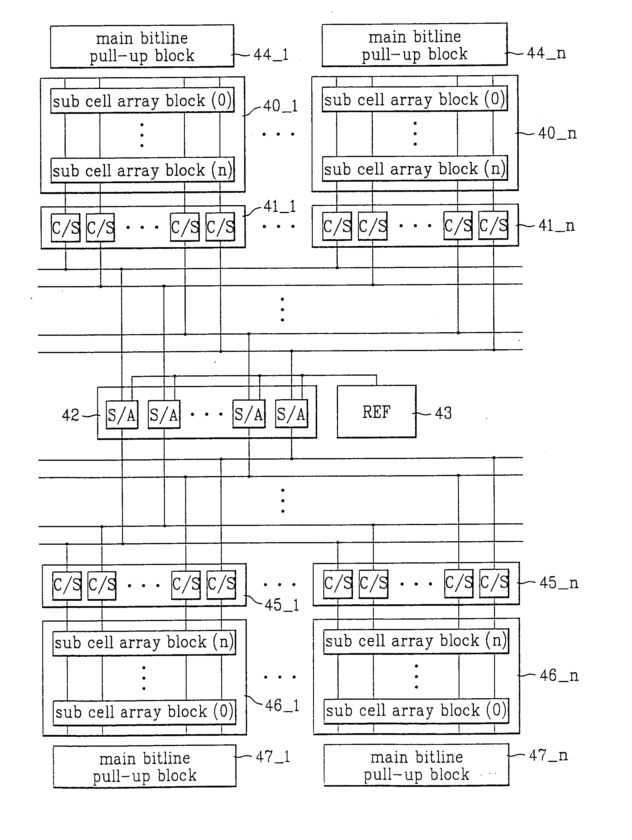
[0062] In the invention's nonvolatile ferroelectric memory device and a method for writing and reading multiple-bit, multiple-bit data is written and read in a cell of FRAM.

[0063] Since voltage dependence is high in a write mode operation, multiple-bit data is stored in a cell by using the...


PUM


Abstract

A nonvolatile ferroelectric memory device and a method for writing and reading multiple-bit data using the same, in which multiple bit data is stored in one cell to reduce a cell layout area, thereby obtaining price competitiveness of a chip. The nonvolatile ferroelectric memory device includes a sensing amplifier block having multiple sensing amplifiers comparing multiple-level signals from main bitlines and sensing them in a multiple-bit, the sensing amplifiers being commonly used in a multiple cell array blocks to feed the sensed multiple-bit levels back and restore them in a cell, and switching transistors arranged one by one per sub bitline to sense data values of the unit cell.

Description

[0001] This application is a Divisional of co-pending application Ser. No. 10 / 317,150, filed on Dec. 12, 2002, the entire contents of which are hereby incorporated by reference and for which priority is claimed under 35 U.S.C. § 120. This application also claims the benefit of Korean Application No. P2001-78928 filed on Dec. 13, 2001, which is hereby incorporated by reference.BACKGROUND OF THE INVENTION [0002] 1. Field of the Invention [0003] The invention pertains to a semiconductor memory, and more particularly, to a nonvolatile ferroelectric memory device and a method for storing a multiple bit using the same. [0004] 2. Discussion of the Related Art [0005] Generally, a nonvolatile ferroelectric memory, i.e., a ferroelectric random access memory (FRAM) has a data processing speed equal to that of a dynamic random access memory (DRAM) and retains data even when the power is off. For this reason, the nonvolatile ferroelectric memory has received much attention as a next generation m...

Claims


Application Information

Patent Timeline
IPC IPC(8): G11C11/22G11C11/56
CPCG11C7/06G11C11/5657G11C11/22
Inventor KANG, HEE BOK
Owner SK HYNIX INC
Why Eureka
Eureka Blog
Learn More