

Thin film magnetic memory device having redundant configuration
- Summary
- Abstract
- Description
- Claims
- Application Information
AI Technical Summary
Benefits of technology
Problems solved by technology
Method used
Image

Examples
first embodiment
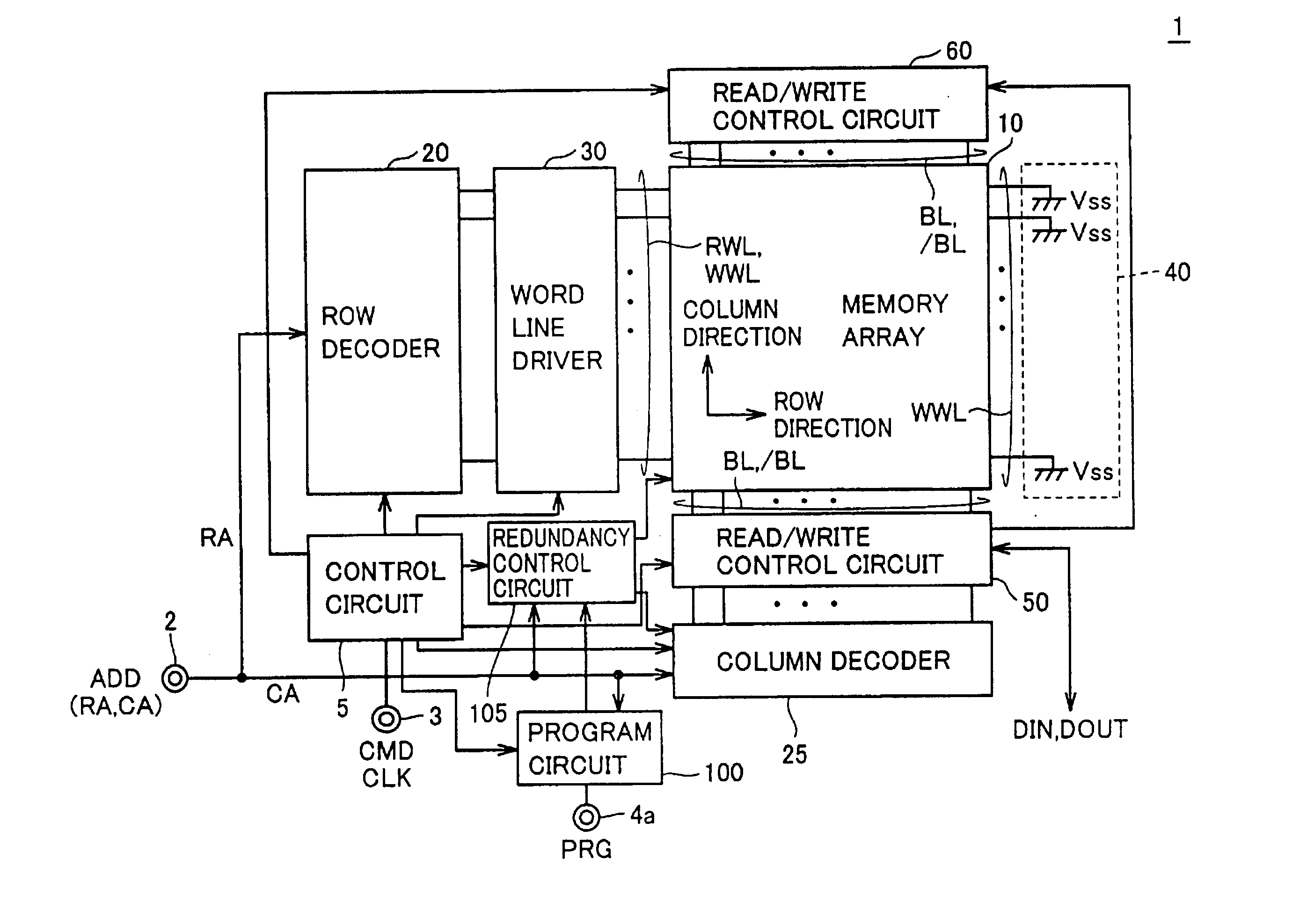
Referring to FIG. 1, the MRAM device 1 according to the first embodiment of the present invention performs random access in accordance with externally applied control signal CMD and address signal ADD, and performs input of write data DIN and output of read data DOUT. The data read operation and the data write operation in MRAM device 1 are performed at timings in synchronization with an externally applied clock signal CLK, for example. Alternatively, the operating timings may be determined within the device, unprovided with external clock signal CLK.
MRAM device 1 includes: an address terminal 2 receiving input of address signal ADD; a control signal terminal 3 receiving input of control signal CMD and clock signal CLK; a signal terminal 4a receiving input of a program signal PRG that is activated in a program operation; a control circuit 5 for controlling the entire operations of MRAM device 1 in response to control signal CMD and clock signal CLK; and a memory array 10 having a pl...
third modification
of First Embodiment
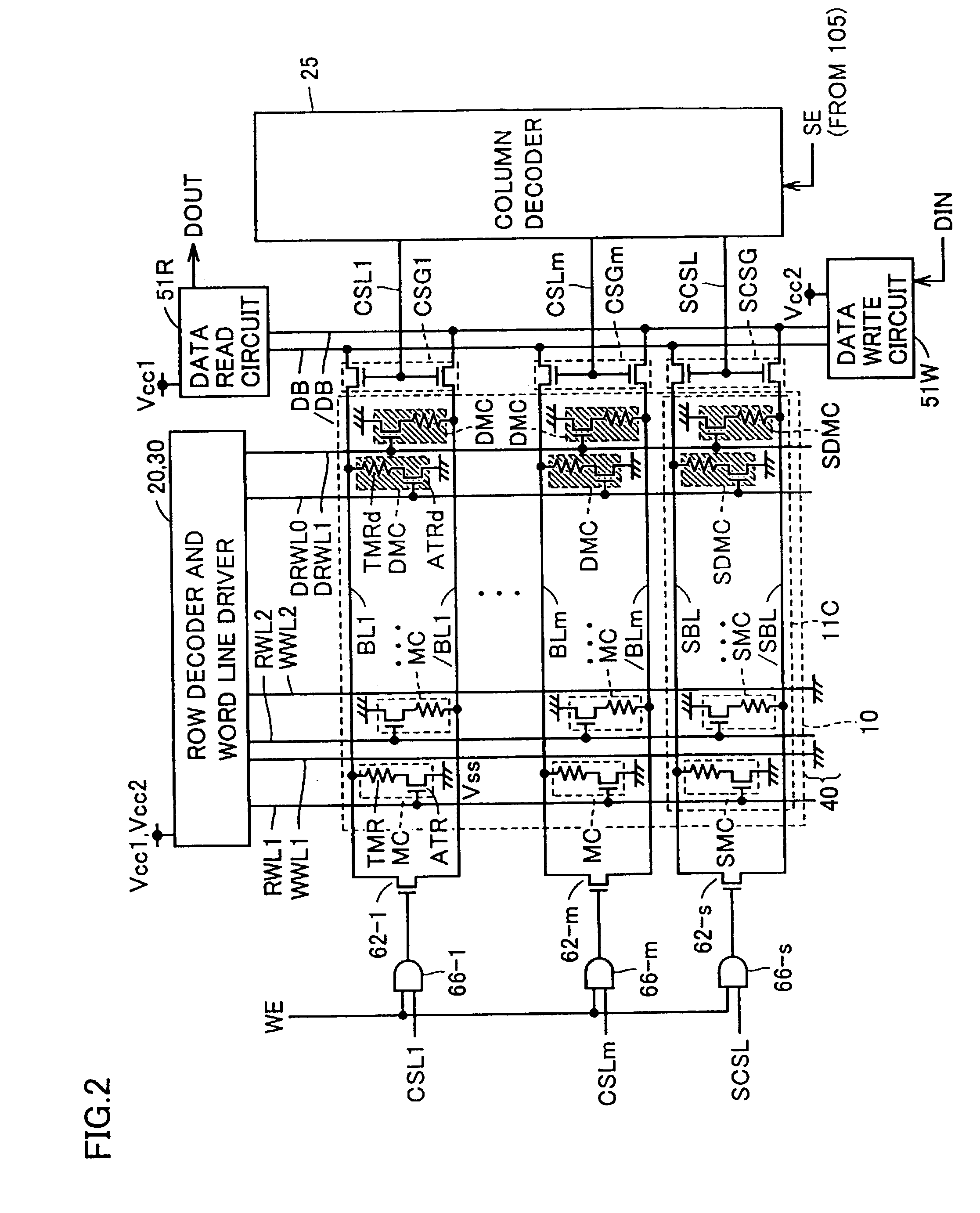
Referring to FIG. 7, in the configuration of the memory array according to the third modification of the first embodiment, memory array 10 is divided to two memory blocks MBa and MBb, each having m normal memory cell columns and a redundant column 11C.
In memory block MBa, bit lines BL1-BLm are arranged corresponding to the m normal memory cell columns, and spare bit line SBL is arranged corresponding to redundant column 11C. Dummy memory cells DMC are arranged one for each memory cell column, and connected to respective bit lines BL1-BLm.
Redundant column 11C has spare memory cells SMC for replacement / repair of normal memory cells MC and spare dummy memory cell SDMC for replacement / repair of dummy memory cell DMC arranged in the column direction. Spare memory cells SMC are arranged to share the memory cell rows with normal memory cells MC. Spare dummy memory cell SDMC is arranged to form a dummy memory cell row with dummy memory cells DMC. Spare memory cells SMC an...
second embodiment
In the second embodiment of the present invention, an efficient way of replacing dummy memory cells in the case where each dummy memory cell is designed to have the same configuration and characteristics as a normal memory cell is described.
FIG. 8 is a circuit diagram showing a memory array configuration and a configuration for reading data from the relevant memory array according to the second embodiment.
Referring to FIG. 8, in the configuration according to the second embodiment, normal memory cells MC and dummy memory cells DMC# in alternate rows are connected to complementary bit lines BL and / BL based on the folded bit line configuration, as in the memory array configuration shown in FIG. 2. Specifically, in the configuration shown in FIG. 8, compared to the arrangement of normal memory cells MC and dummy memory cells DMC shown in FIG. 2, dummy memory cells DMC# replacing dummy memory cells DMC are arranged to form dummy memory cell rows. Dummy memory cells DMC# each having the...
PUM
 Abstract
Description
Claims
Application Information