Multi-layer PCB and method for coupling block type multichannel optical signals

a multi-layer printed circuit board and coupling block technology, applied in the field of multi-layer printed circuit boards and coupling block type multi-channel optical signals, can solve the problems of alignment errors between limited wavelength of optical signals that can be transmitted through conventional multi-layer pcbs, and inability to disclose the technique for inserting optical waveguides into multiple layers of multi-layer pcbs. achieve the effect of reducing physical impa

Inactive Publication Date: 2005-12-20
SAMSUNG ELECTRO MECHANICS CO LTD
View PDF4 Cites 7 Cited by
  • Summary
  • Abstract
  • Description
  • Claims
  • Application Information

AI Technical Summary

Benefits of technology

[0039]Preferably, the multi-layer PCB may further comprise a packaging frame attached to enclose the base boards and the optical waveguides

Problems solved by technology

However, the conventional multi-layer PCB using the optical via holes 16 to transmit the optical signal 19 is problematic in that the micro lens 17 must be used, and the wavelength of an optical signal that can be transmitted through the conventional multi-layer PCB is limited to 200 μm.
Additionally, a technique for inserting optical waveguides into the multiple layers of a multi-layer PCB has not been disclosed.
However, the

Method used


Image

  • Multi-layer PCB and method for coupling block type multichannel optical signals
  • Multi-layer PCB and method for coupling block type multichannel optical signals
  • Multi-layer PCB and method for coupling block type multichannel optical signals

Examples


first embodiment

[0082]A first embodiment of the present invention relates to a method of sequentially coupling block type multichannel optical signals in a multi-layer PCB.

[0083]FIGS. 6a and 6b are plan views of a fixing guide and the fixing guide attached to a base board, respectively.

[0084]Referring to FIGS. 6a and 6b, windows J, which have sizes corresponding to those of optical signal connection blocks 86 to be inserted therein and are formed at positions corresponding to those of optical via holes, are formed in a fixing guide 85. In this case, the fixing guide 85 may be made of a silicon board or polymer material. Thereafter, optical fibers or optical waveguides are inserted into the optical signal coupling block 86.

[0085]FIGS. 7a to 7g are views showing a method of inserting optical waveguides and fiber or pipe blocks into a multi-layer base board according to a first embodiment of the present invention.

[0086]FIG. 7a is a plan view showing a structure on which a fixing guide with windows for...

second embodiment

[0095]A second embodiment of the present invention relates to a multi-layer PCB and method for simultaneously coupling block type multichannel optical signals.

[0096]FIGS. 8a to 8g are views showing a method of inserting optical waveguides and fiber or pipe blocks in a multi-layer PCB according to a second embodiment of the present invention.

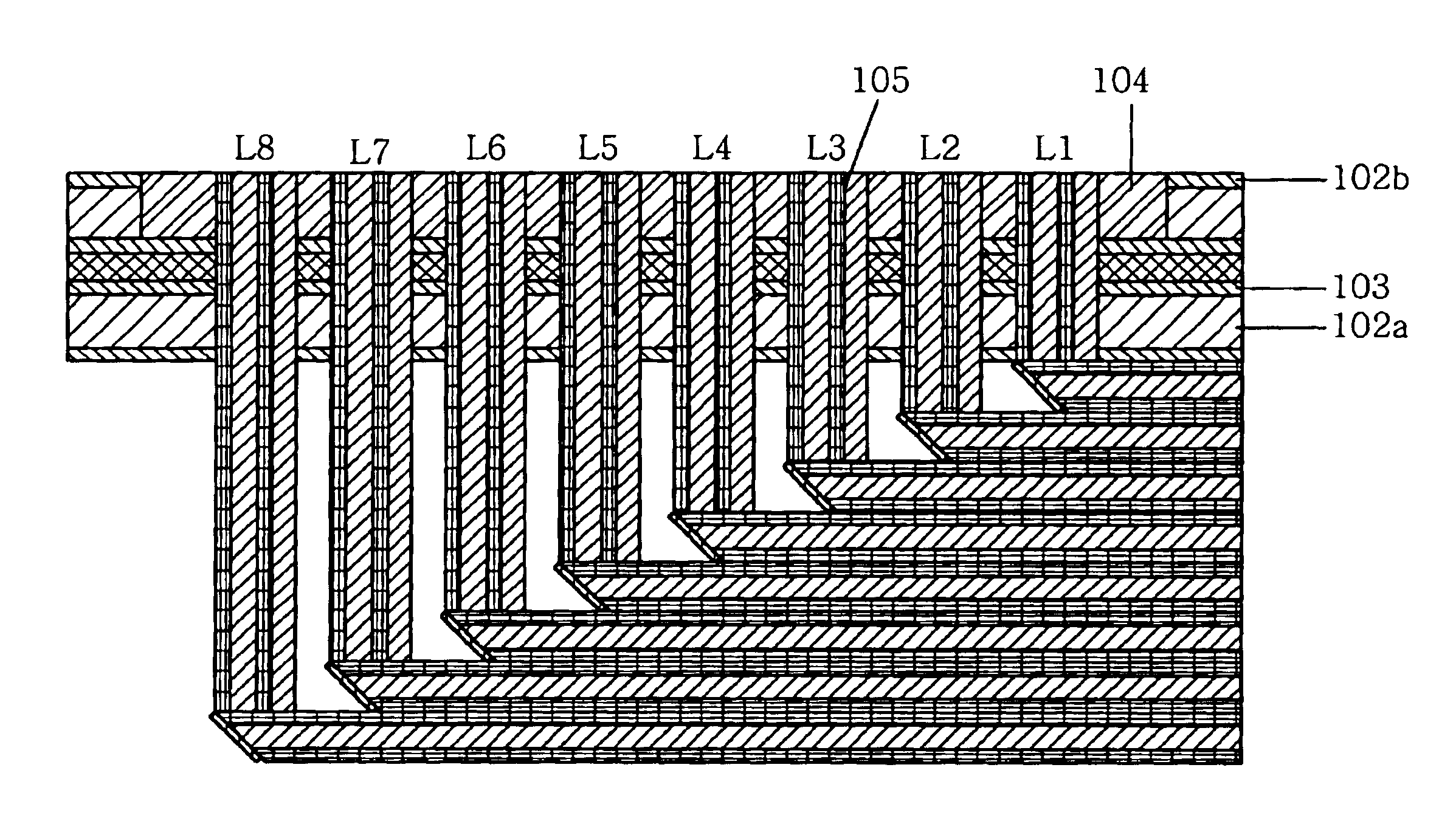
[0097]FIG. 8a is a plan view showing a structure in which a fixing guide with windows formed therein is attached to a base board. Referring to FIG. 8a, a fixing guide 100, in which a plurality of windows L are formed to allow optical signal coupling blocks to be inserted therein, is attached to a base board. In fact, FIG. 8a is a plan view showing a structure that has undergone the steps illustrated in FIGS. 8b to 8d.

[0098]In order to implement the multi-layer PCB and method for coupling block type multichannel optical signals in accordance with the second embodiment of the present invention, a plurality of optical via holes L1 to L8 are formed ...


PUM


Abstract

The present invention discloses a multi-layer Printed Circuit Board (PCB) and method for coupling block type multichannel optical signals, the method including the steps of i) forming one or more first optical via holes to allow one or more first optical signal coupling blocks to be inserted therein, ii) aligning a first optical waveguide and the first optical signal coupling blocks so that the first optical waveguide is interconnected to the first optical signal coupling blocks via an optical signal, iii) attaching a first fixing guide to a base board to fasten the first optical signal coupling blocks, iv) removing the first fixing guide and forming one or more second optical via holes to allow one or more second optical signal coupling blocks to be inserted therein, and v) repeatedly performing steps i) to iv) as many times as a number of layers of the multi-layer PCB.

Description

BACKGROUND OF THE INVENTION[0001]1. Field of the Invention[0002]The present invention relates generally to a multi-layer printed circuit board and method for coupling block type multichannel optical signals, and more particularly to a multi-layer printed circuit board and method for coupling block type multichannel optical signals, in which a plurality of optical via holes are formed in a multi-layer base board, fiber or pipe blocks are simultaneously or sequentially inserted into the optical via holes through the use of fixing guides, and optical waveguides and optical fibers are interconnected to one another between layers, thereby forming N×N block type multichannel optical waveguides in multiple layers instead of conventional 1×N block type multichannel optical waveguides.[0003]2. Description of the Prior Art[0004]Generally, a Printed Circuit Board (PCB) is a circuit board fabricated by densely mounting a plurality of components on a plate made of phenol resin or epoxy resin and...

Claims


Application Information

Patent Timeline
IPC IPC(8): G02B6/36H05K3/46G02B6/43
CPCG02B6/43G02B6/3652G02B6/3676G02B6/3688G02B6/3692H05K3/46
Inventor KIM, YOUNG-WOORHEE, BYOUNG-HOYANG, DEK-GINCHOYIM, KYU-HYOK
Owner SAMSUNG ELECTRO MECHANICS CO LTD
Why Eureka
Try Eureka