Manufacturing method and dismantling method for plasma display device

Inactive Publication Date: 2005-12-27
PANASONIC CORP
View PDF3 Cites 19 Cited by
  • Summary
  • Abstract
  • Description
  • Claims
  • Application Information

AI Technical Summary

Benefits of technology

[0016]This configuration can easily separate a panel, made mainly of glass, from a chassis, made mainly of metal, by cutting

Problems solved by technology

On the other hand, a glass panel of a plasma display device must necessarily be easily separated from a metal chassis for scrapping and recycli

Method used


Image

  • Manufacturing method and dismantling method for plasma display device
  • Manufacturing method and dismantling method for plasma display device
  • Manufacturing method and dismantling method for plasma display device

Examples


Embodiment Construction

[0028]Exemplary embodiments of this invention are described with reference to the drawings.

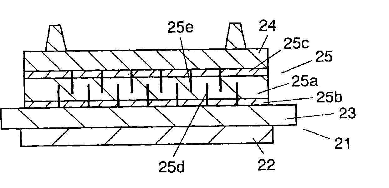
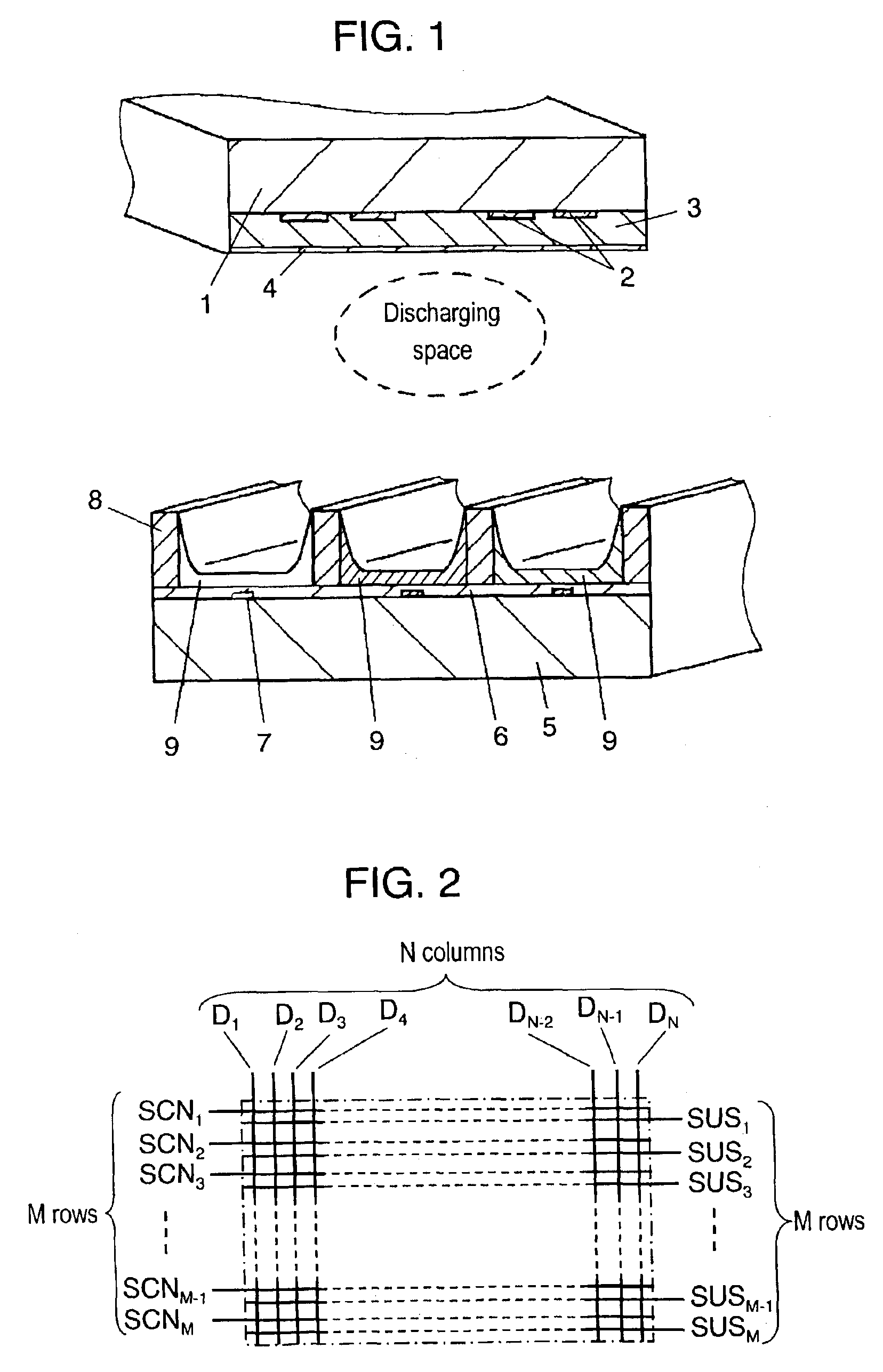
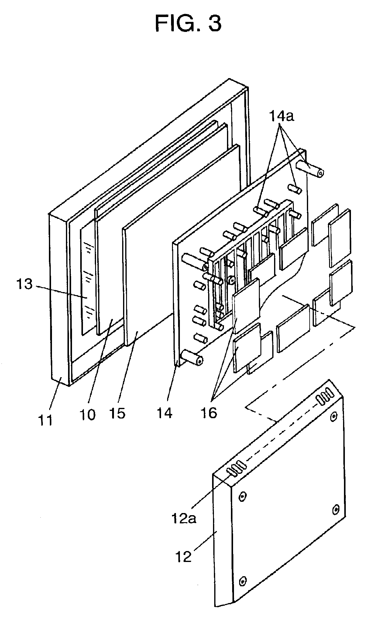
[0029]First, a plasma display device is described using FIGS. 1 to 3.

[0030]FIG. 1 illustrates a perspective view showing a panel structure of a plasma display device.

[0031]A panel has following structures:

[0032](a) a plurality of arrays of display electrodes 2 consists of pairs of a scan electrode and a sustain electrode formed on transparent front substrate 1;

[0033](b) dielectric layer 3 formed on the arrays of electrodes to cover the electrodes;

[0034](c) protective layer 4 formed on dielectric layer 3 to cover the dielectric layer;

[0035](d) a plurality of arrays of stripe shaped address electrodes 7 covered by overcoat layer 6 formed on rear substrate 5, which is placed facing front substrate 1, with the address electrodes crossing display electrodes 2 consisting of scan electrodes and sustain electrodes;

[0036](e) a plurality of ribs 8 placed in parallel with address electrodes 7;

[0037](f) f...


PUM

PropertyMeasurementUnit
Thicknessaaaaaaaaaa
Lengthaaaaaaaaaa
Electrical conductoraaaaaaaaaa

Abstract

A manufacturing method and dismantling method of a plasma display device are disclosed. These methods can bond a panel to a holder reliably, and can separate the panel and holder easily upon scrapping a plasma display device. The manufacturing method comprises steps of: (a) bonding one of adhesive layers, which are provided on both surfaces of an adhesive sheet consisting of a porous insulating sheet, to a panel holder, to bond a rear surface of a panel to the holder, and (b) bonding another adhesive layer to a rear surface of the panel. And, the dismantling method comprises the step of separating the panel from the holder by cutting the porous insulating sheet of the adhesive sheet.

Description

TECHNICAL FIELD[0001]The present invention relates to a manufacturing method for a plasma display device, and a dismantling method for scrapping the plasma display device, known as a technology for a large screen with slim and lightweight display.BACKGROUND ART[0002]Recently, a plasma display device (thin display panel) has become an attractive subject as a display with excellent visibility, and this technology is steadily advancing for large-sized screens with high definition.[0003]Such plasma display devices are roughly divided into AC powered and DC powered in terms of a driving method, and surface discharge and counter discharge in terms of a discharging method. Currently, however, surface discharge AC powered structure has become a mainstream technology from a stand point of high definition, large screen and simplified manufacturing.[0004]In the field of plasma display device technology, an example is disclosed in Japanese Patent No. 2,807,672 to bond together a panel, made mai...

Claims


Application Information

Patent Timeline
IPC IPC(8): H01J9/52H01J9/24H01J11/34
CPCH01J9/52Y10T156/1184Y10T156/1052H01J2217/49Y02W30/82H01J9/24H01J11/34
Inventor WATANABE, HIROSHI
Owner PANASONIC CORP
Why Eureka
Try Eureka