Screening device for electronic subassemblies on a printed circuit board

a technology of electronic sub-assemblies and printed circuit boards, applied in the direction of screening gaskets/seals, localised screening, screening casings, etc., can solve the problems of time-consuming assembly, interference radiation can also be caused, cumbersome process, etc., and achieve the effect of reducing costs

Inactive Publication Date: 2005-12-27
UNIFY GMBH & CO KG
View PDF6 Cites 37 Cited by
  • Summary
  • Abstract
  • Description
  • Claims
  • Application Information

AI Technical Summary

Benefits of technology

[0008]The underlying object of the invention is to develop a screening device of the type stated at the start which improves screening efficiency and makes it possible to manufacture screening devices, especially those of different sizes, with less effort.

Problems solved by technology

On printed circuit boards the interference radiation can also be caused by subassemblies located on the same printed circuit board.
Putting the cover on and taking it off is a cumbersome process and assembly is time-consuming.
Under harsh operating conditions it can occur that contacting fails as a result of mechanical effects or corrosion.
In this case the screening efficiency of the interference suppression medium is adversely affected.
A further disadvantage is that a compression force is necessary on assembly of the screening cover to overcome the spring pressure, said force having to be applied to the screen tray and borne by the printed circuit board.
Micro cracks can then develop in the conductive structure.
Manufacturing these known one-piece screening devices requires a complex manufacturing tool.
Changes to this tool required to produce a new screening geometry or spatial form are only possible with a comparatively large amount of effort.

Method used


Image

  • Screening device for electronic subassemblies on a printed circuit board
  • Screening device for electronic subassemblies on a printed circuit board
  • Screening device for electronic subassemblies on a printed circuit board

Examples


Embodiment Construction

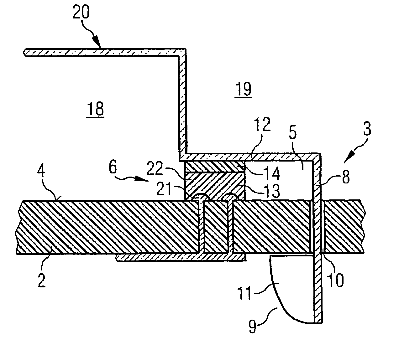
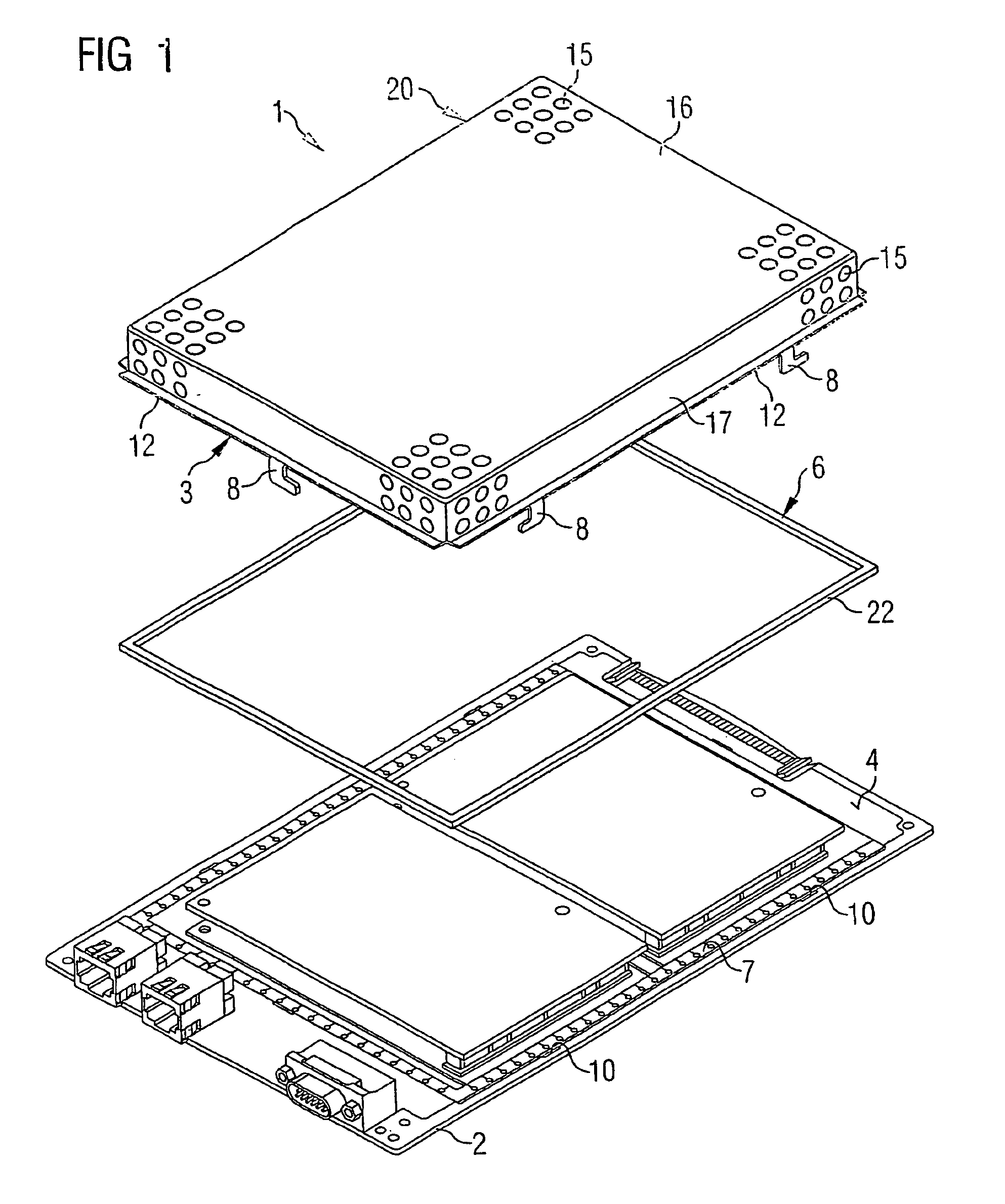
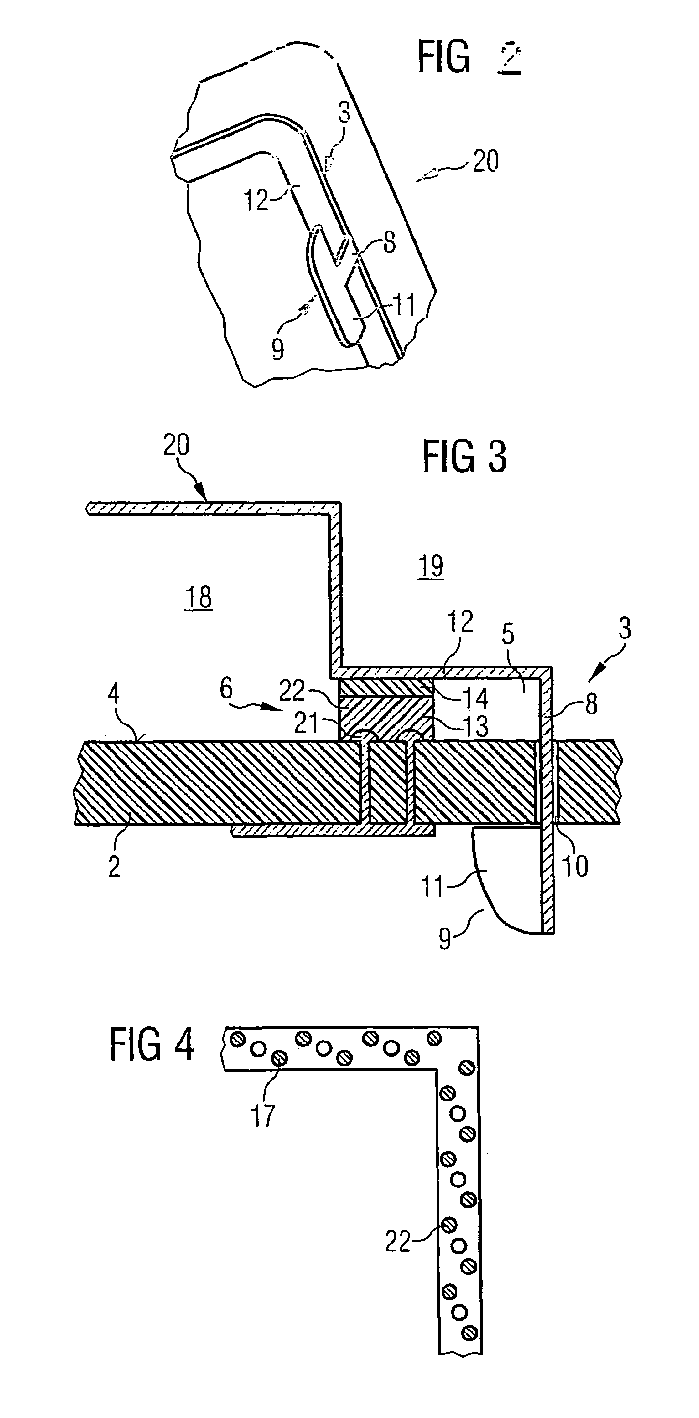
[0028]In the drawings FIG. 1 shows a typical embodiment of the inventive screening device 1 in an exploded perspective view. The screening device 1 consists of a screening cover 20 and a contact device 6. In the example shown, the screening cover 20 covers the entire area of the printed circuit board 2. The explanations below are not however restricted to this embodiment but in particular also include screening devices which cover only parts of the printed circuit board.

[0029]As shown in FIG. 1 lugs 8 are formed on the outer edge 3 of the screening cover by which the screening cover 20 can be attached to a component side 4 of the printed circuit board 2. On the component side 4 of the printed circuit board 2 a guide contour 7 can be seen of which the outline corresponds to the edge area of the screening cover 20. The guide contour 7 consists of contact points which are explained in greater detail below and is etched to correspond to the pitch of the board. The contact device 6 is em...


PUM


Abstract

The invention relates to a screening device comprising: a screening cover, which covers an electronic circuit located on a printed circuit board and comprises an edge that is separated from the component side of the printed circuit board by a gap and a contact device, which is located in the gap and produces an electric connection between the screening cover and a conductive contour element on the printed circuit board. According to the invention, lugs are formed on the edge of the screening cover, said lugs fixing the screening cover on the printed circuit board and maintaining an elastic pretension on the contact device. The contact device is configured as an elastic sealing body that extends continuously through the gap and absorbs electromagnetic waves.

Description

CROSS REFERENCE TO RELATED APPLICATIONS[0001]This application is the US National Stage of International Application No. PCT / EP2003 / 005182, filed May 16, 2003 and claims the benefit thereof. The International Application claims the benefits of German application No. 10231145.5 filed Jul. 10, 2002, both applications are incorporated by reference herein in their entirety.FIELD OF THE INVENTION[0002]The invention relates to a screening or shielding device with a screening cover which covers an electronic circuit located on a printed circuit board, with an edge that is separated from the component side of the printed circuit board by a gap and a contact device which is located in the gap and produces an electrical connection between the screening cover and a conducting contour element on the printed circuit board, with lugs being formed on the edge of the screening cover by which the screening cover is fixed to the printed circuit board and maintaining an elastic pretension on the screen...

Claims


Application Information

Patent Timeline
Patent Type & Authority Patents(United States)
IPC IPC(8): H05K9/00
CPCH05K9/0015H05K9/0028H05K9/003
Inventor FURSICH, WALTER
Owner UNIFY GMBH & CO KG
Why Eureka
Try Eureka