Semiconductor device and method of manufacturing same

a semiconductor device and semiconductor technology, applied in the direction of semiconductor devices, semiconductor/solid-state device details, electrical devices, etc., can solve the problems of increasing the cost of semiconductor devices, difficult to sufficiently increase the area, and limiting the improvement of heat dissipation characteristics, so as to reduce peeling, and improve heat dissipation characteristics

Inactive Publication Date: 2005-12-27
MITSUBISHI ELECTRIC CORP
View PDF23 Cites 52 Cited by
  • Summary
  • Abstract
  • Description
  • Claims
  • Application Information

AI Technical Summary

Benefits of technology

[0031]In the semiconductor device of the fifth aspect or the sixth aspect of the present invention, the formation of the insulation space between the metal block and the lead frame enables the metal block to be sized to horizontally extend to near the outline of the semiconductor device. This enhances the heat dissipation characteristic.
[0032]In the method of manufacturing the semiconductor device of the seventh aspect of the present invention, the simultaneous curing of the insulation layer and the resin package reduces peeling at an interface between the different resins. Consequently, the dielectric breakdow...

Problems solved by technology

This gives rise to a limit to the improvement in the heat dissipation characteristic.
This causes the needless use of the costly resin, to increase the cost of the materials of the semiconductor device.
It has therefore been difficult to sufficiently increase the area over which heat passes through the resin...

Method used


Image

  • Semiconductor device and method of manufacturing same
  • Semiconductor device and method of manufacturing same
  • Semiconductor device and method of manufacturing same

Examples


Embodiment Construction

[0046]First Preferred Embodiment

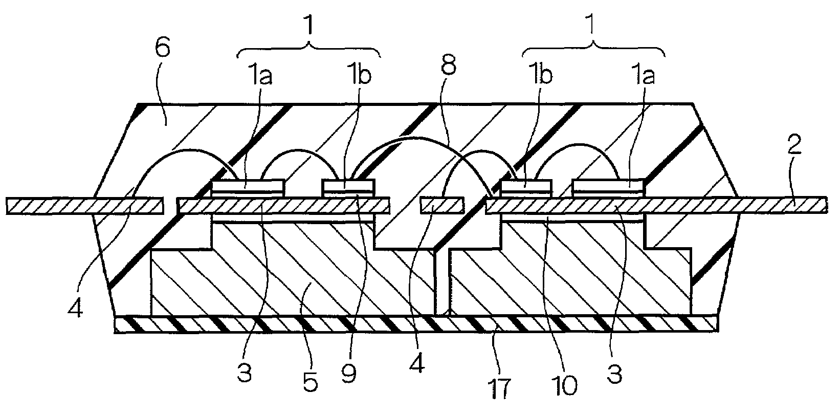
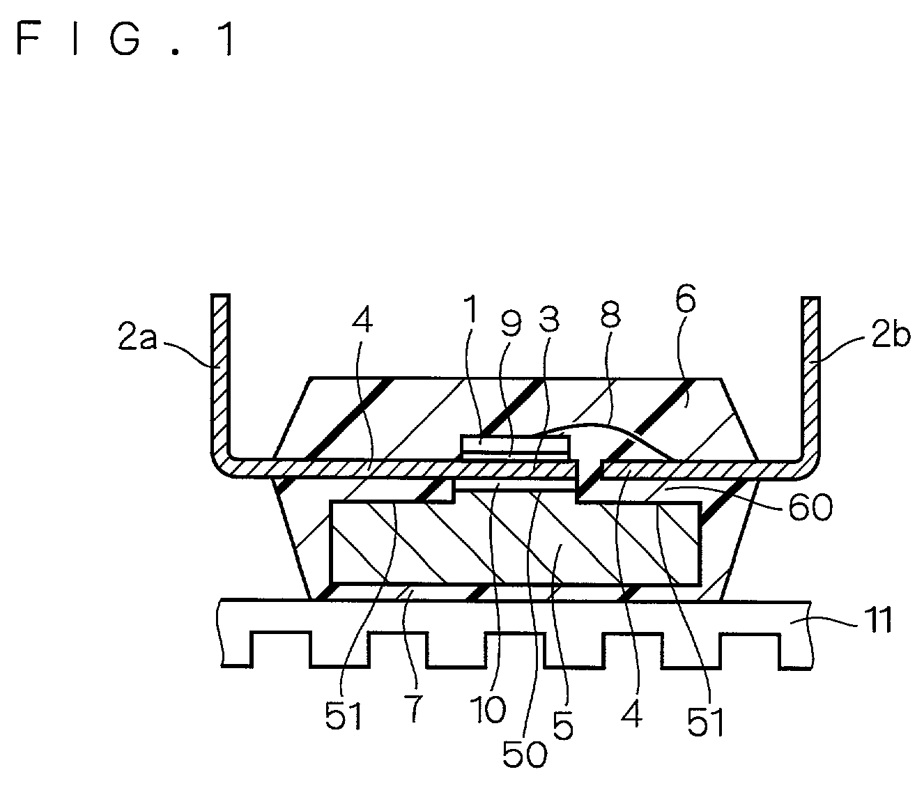
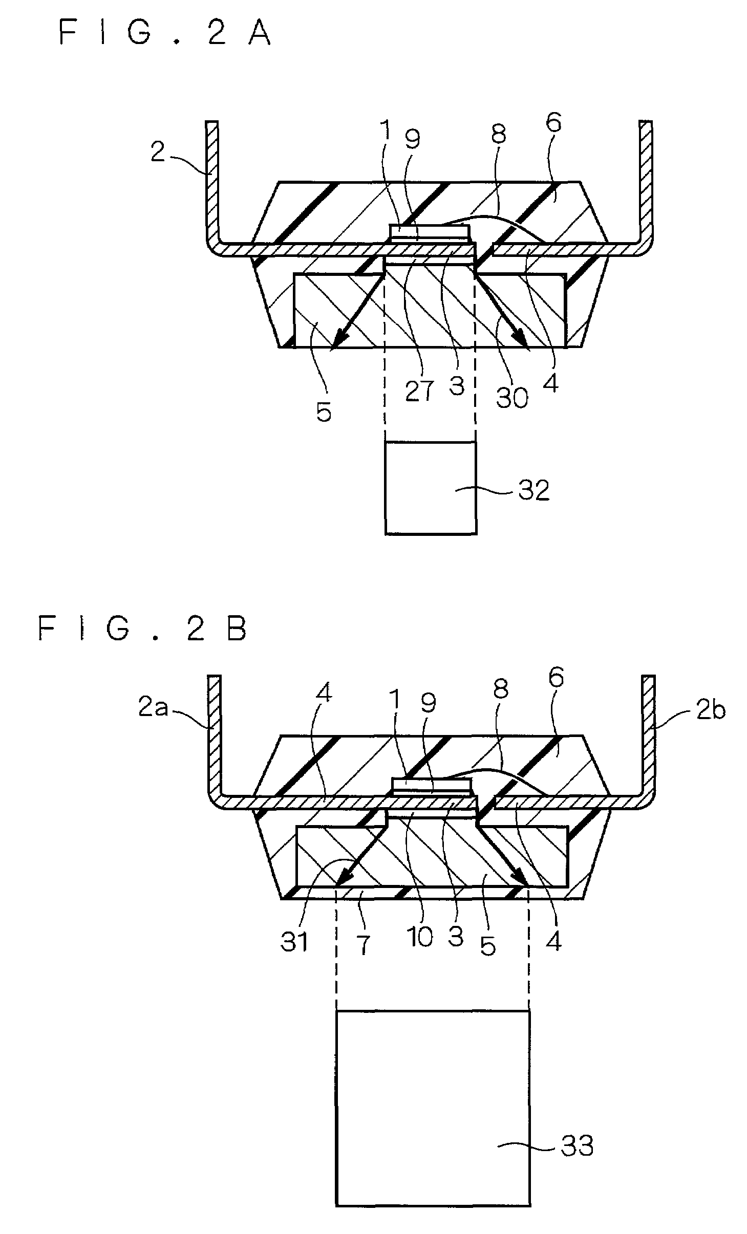
[0047]FIG. 1 is a schematic sectional view of a structure of a semiconductor device according to a first preferred embodiment of the present invention. As shown in FIG. 1, the semiconductor device according to the first preferred embodiment comprises a power semiconductor element (referred to hereinafter as a power element) 1, lead frames 2a and 2b, a metal block 5, and a resin package 6.

[0048]The lead frames 2a and 2b are formed from a sheet of metal having good thermal conductivity, e.g., a copper alloy. The lead frame 2a has a die bonding pad portion 3 and an inner lead portion 4, and the lead frame 2b has an inner lead portion 4. The power element 1 has first and second electrodes (not shown) on first and second surfaces thereof, respectively. The power element 1 is mounted on the die bonding pad portion 3 of the lead frame 2a and is bonded to the die bonding pad portion 3 with solder 9 so that the first electrode on the first surface thereof cont...


PUM


Abstract

A lead frame (2a) has a die bonding pad portion (3) and an inner lead portion (4). A power element (1) is mounted on the die bonding pad portion (3) of the lead frame (2a) and is bonded to the die bonding pad portion (3) with solder (9). The power element (1) has electrodes connected through an aluminum wire (8) to the inner lead portion (4) of another lead frame (2b). A metal block (5) has a surface formed with a protrusion bonded to the lead frame (2a) in opposed relation to the power element (1). A resin package (6) has an insulation layer (7) formed on the opposite surface of the metal block (5) from the lead frame (2a), and seals the power element (1), the lead frames (2a, 2b) and the metal block (5). An external heat dissipator (11) is mounted on a surface of the insulation layer (7) opposite from the metal block (5). A semiconductor device and a method of manufacturing the same improve a heat dissipation characteristic and maintain a dielectric breakdown voltage.

Description

BACKGROUND OF THE INVENTION[0001]1. Field of the Invention[0002]The present invention relates to a structure of a semiconductor device and, more particularly, to a structure of a power semiconductor device for use in power control and a method of manufacturing the same.[0003]2. Description of the Background Art[0004]FIG. 8 is a schematic sectional view of a structure of a first background art power semiconductor device. As shown in FIG. 8, the first background art power semiconductor device comprises a power element 1, lead frames 2 formed from sheet metal, a metal block 5 functioning as a heat sink for heat dissipation, and a resin package 6.[0005]The lead frames 2 have a die bonding pad portion 3 and an inner lead portion 4. The power element 1 is bonded to the die bonding pad portion 3 with solder 9. The power element 1 is formed with electrodes (not shown) connected to the inner lead portion 4 of one of the lead frames 2 through an aluminum wire 8. The metal block 5 has a protru...

Claims


Application Information

Patent Timeline
IPC IPC(8): H01L23/433H01L23/29H01L23/495H01L23/50H01L25/04H01L25/07H01L25/18
CPCH01L23/4334H01L23/49575H01L24/49H01L24/45H01L2224/32245H01L2224/45124H01L2224/48091H01L2224/48137H01L2224/48247H01L2224/4911H01L2224/73265H01L2924/01004H01L2924/01005H01L2924/01006H01L2924/01013H01L2924/01014H01L2924/01015H01L2924/0102H01L2924/01029H01L2924/01074H01L2924/01082H01L2924/13055H01L2924/1532H01L2924/00014H01L24/48H01L2924/01023H01L2924/01033H01L2924/01068H01L2924/014H01L2924/15747H01L2924/00H01L2224/48139H01L2924/181H01L2224/49111H01L2224/49113H01L2224/48096H01L2924/00012H01L25/04
Inventor SHINOHARA, TOSHIAKI
Owner MITSUBISHI ELECTRIC CORP
Why Eureka
Try Eureka