Double-sided thermally enhanced IC chip package

a chip package and integrated circuit technology, applied in the direction of electrical equipment, semiconductor devices, semiconductor/solid-state device details, etc., can solve the problems of thermal capability, complex and expansive process to implement an integral heat sink into the substrate, and cyclical temperature differences that exaggerate differences in expansion

Inactive Publication Date: 2005-02-01
UTAC HEADQUARTERS PTE LTD
View PDF8 Cites 32 Cited by
  • Summary
  • Abstract
  • Description
  • Claims
  • Application Information

AI Technical Summary

Benefits of technology

It is therefore the primary objective of the present invention to provide a double-sided thermally enhanced IC chip package which is free from the drawbacks of the prior art IC chip package.

Problems solved by technology

Thus, there are likely to be cyclical temperature differences that exaggerate differences in expansion due to differences in coefficient of thermal expansion.
Moreover, the processes to implement an integral heat sink into the substrate are relatively complex and expansive.
Besides, there will have some problems on thermal capability when applying the above IC chip package to a stacked IC chip package, such as an embodiment disclosed in U.S. Pat. No.6,380,615, the upper chip stacked on the other chip might not reach an efficient heat dissipation.

Method used


Image

  • Double-sided thermally enhanced IC chip package
  • Double-sided thermally enhanced IC chip package
  • Double-sided thermally enhanced IC chip package

Examples


first embodiment

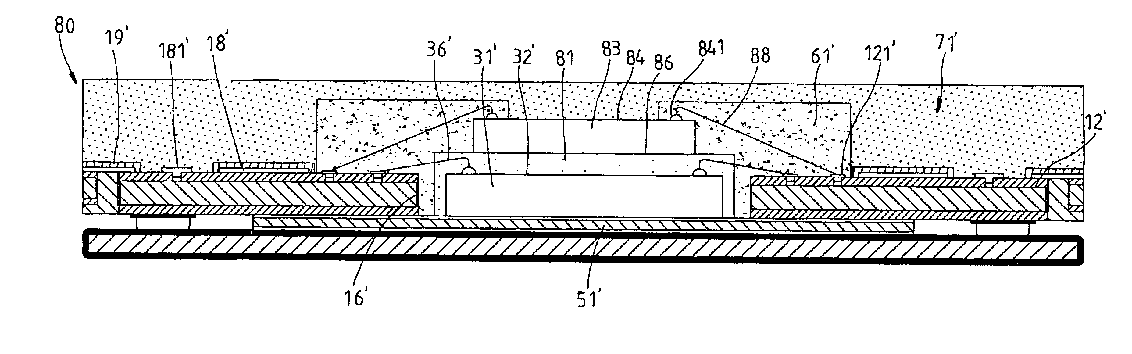
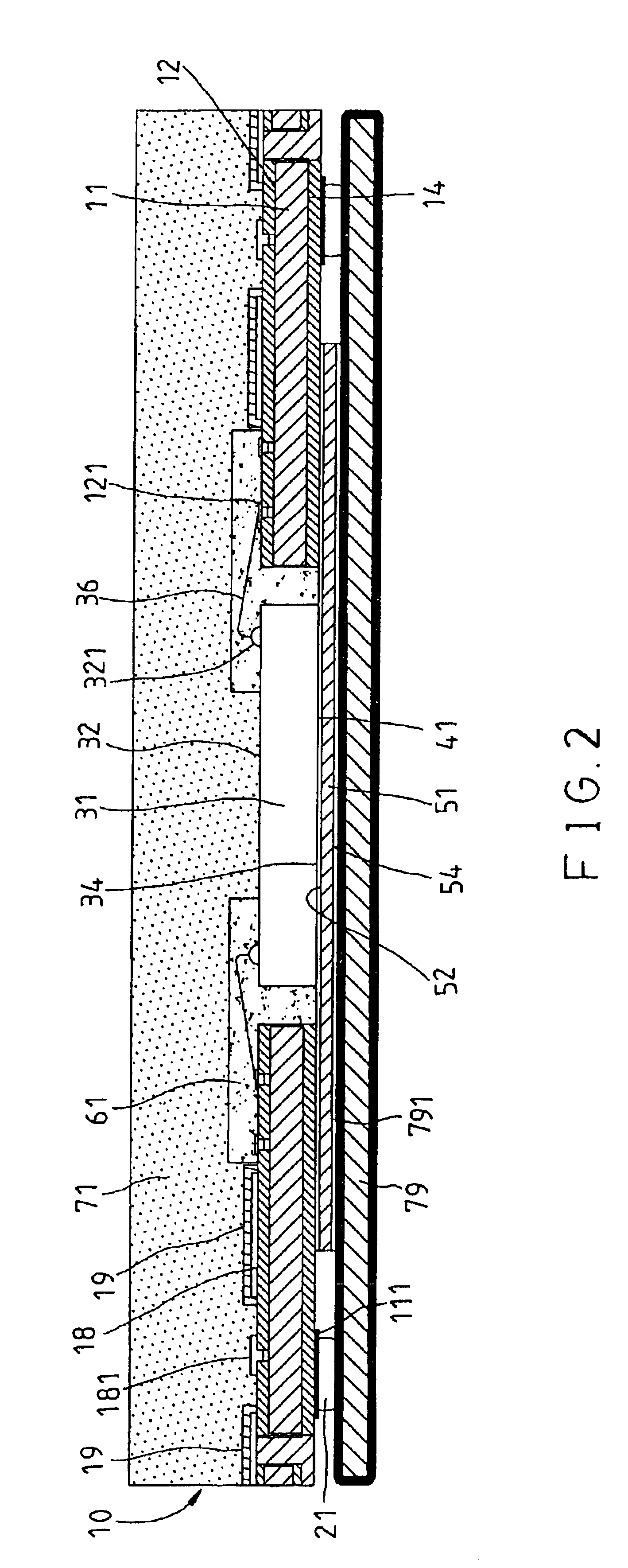
As shown in FIGS. 1-3, there depict a package 10 within the present invention. The package 10 includes a substrate or board 11 made of a suitable dielectric, or insulative, material such as fiberglass reinforced epoxy resin. The substrate 11 has a top and bottom surfaces 12, 14 on which a conductive circuit pattern 18 is respectively laid. The conductive circuit patterns 18 are electrically connected to each other through plated through holes (PTHs). A central window, or opening 16, of a particular size and shape, is formed through the thickness of the substrate 11. A solder mask layer 19 partially covers the circuit pattern 18 on the top surface 12 such that the ground ends 181 of the circuit pattern 18 on the top surface are exposed.

A plurality of solder balls 21 are attached at respective one of the mounting pads 111 of the conductive circuit pattern on the bottom surface 14.

An IC chip 31 has an active side 32 and an inactive side 34. The chip 31 is received in the opening 16. A ...

third embodiment

As shown in FIG. 5, a package 90 of a third preferred embodiment of the present invention is similar to that of the first preferred embodiment except that the third embodiment further comprises a metal foil 91 which covers the solder mask layer 19″. The thermally and electrically conductive encapsulant 71″ encapsulates the metal foil. The metal foil 91 enhances the heat dissipation efficiency of the circuit pattern 18″ on the substrate 11″.

In conclusion, the present invention allows the heat generated by chip in the package being transferred through the thermally and electrically conductive planar member 51, and through the thermally and electrically conductive encapsulant 71 also. The present invention has the effect of heat dissipation by both sides of the package, which is better than the prior art.


PUM


Abstract

The present invention is to provide a double-sided thermally enhanced IC chip package which includes a chip being received in an opening of a substrate and electrically connected to a conductive circuit pattern on a top surface of the substrate through bonding wires. A thermally and electrically conductive planar member is attached to an inactive side of the chip through a thermally and electrically conductive adhesive layer. A portion of an active side of the chip to which the bonding wires are connected is encapsulated by a dielectric encapsulant, and the other portion of the active side of the chip is covered by a thermally and electrically conductive encapsulant. Thus, heat generated by the chip can be efficiently dissipated through the planar member and the thermally and electrically conductive encapsulant. The present invention also discloses a stacked chip package with double-sided heat dissipation capability.

Description

FIELD OF THE INVENTIONThe present invention relates generally to an integrated circuit (IC) chip package, and more particularly to a low cost, high performance IC chip package with enhanced thermal capabilities through two sides.BACKGROUND OF THE INVENTIONU.S. Pat. No.5,355,283 discloses a prior art thermally enhanced IC chip package, which includes a substrate with a central hole. The substrate is bonded to a heat sink, which can be made of copper or other materials having an acceptably high thermal conductivity, by an adhesive such as an epoxy adhesive. An IC chip is also bonded to the heat sink by the adhesive within the central hole, which is subsequently filled with an encapsulant.The presence of the heat sink in such a conventional IC chip package as described above can provide good heat transfer away from the chip, particularly since most of the heat sink surface is exposed to the exterior of the package. However, it has some drawbacks. The differences in coefficient of therm...

Claims


Application Information

Patent Timeline
Patent Type & Authority Patents(United States)
IPC IPC(8): H01L23/28H01L23/31H01L25/065H01L23/36H01L23/433H01L23/498H01L23/29H01L23/48H01L23/34
CPCH01L23/29H01L23/3128H01L23/36H01L23/4334H01L23/49894H01L25/0657H01L2224/45144H01L24/48H01L2924/15311H01L2924/1517H01L2924/15153H01L2924/14H01L2924/01079H01L2924/01029H01L2225/06589H01L2225/06555H01L2225/0651H01L2224/48091H01L2224/48227H01L2224/48465H01L2924/00014H01L2924/00H01L24/45H01L2224/05554H01L2924/10162
Inventor TSAI, CHUNG-CHESHAN, WEI-HENG
Owner UTAC HEADQUARTERS PTE LTD
Why Eureka
Try Eureka