
Method and device for mounting electronic component on circuit board

a technology for electronic components and circuit boards, applied in the direction of printed circuit assembling, printed circuit manufacture, basic electric elements, etc., can solve the problems of high cost, degraded productivity, and difficulty in reducing the size of circuit boards

Inactive Publication Date: 2006-01-03
PANASONIC CORP
View PDF62 Cites 73 Cited by
  • Summary
  • Abstract
  • Description
  • Claims
  • Application Information

AI Technical Summary

Benefits of technology

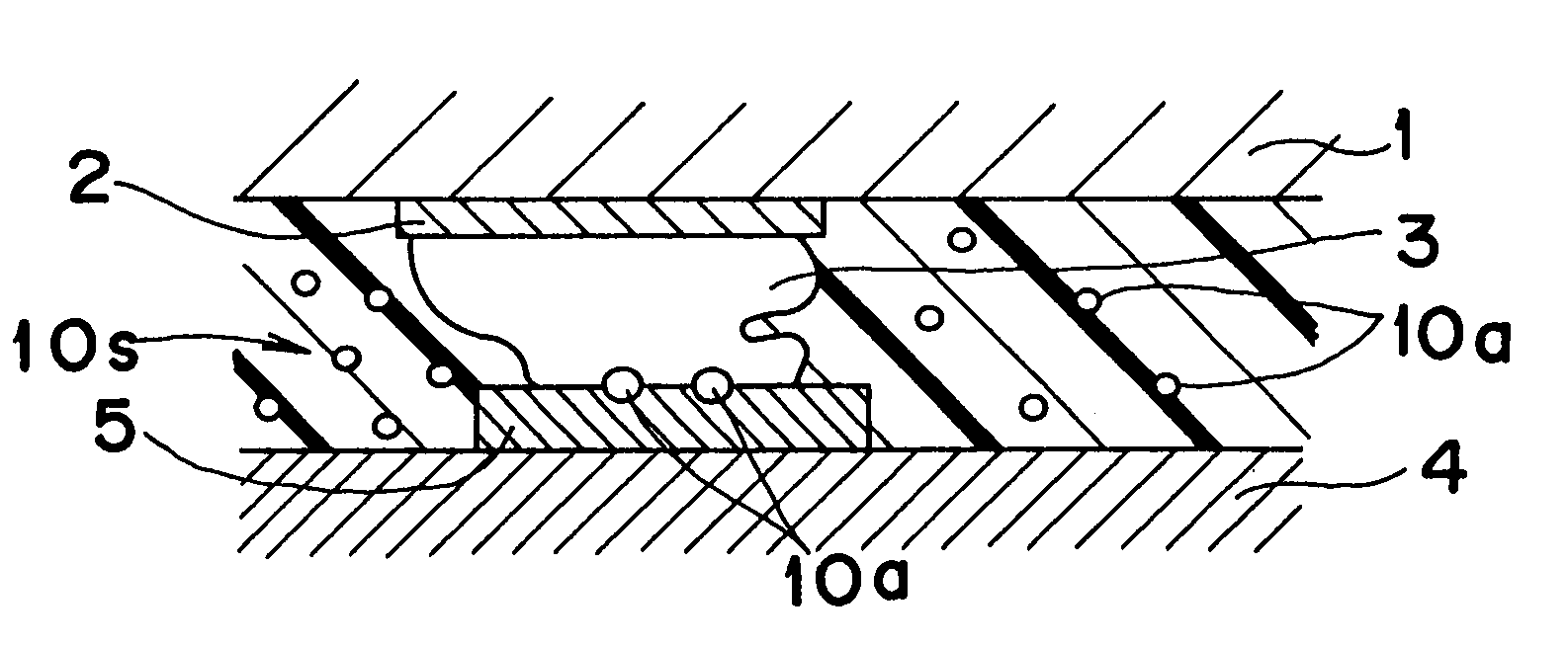
[0040]the bonding device hardens with the heat the thermosetting resin interposed between the electronic component and the circuit board while simultaneously performing leveling of the bumps and correction of the warp of the board by pressurizing the electronic component against the circuit board with the pressure force of not smaller than 20 gf per bump with the heat applied to the thermosetting resin from the heating device, thereby bonding the electronic component and the circuit board together for electrical connection between both the electrodes thereof.

Problems solved by technology

According to the above processing method called SMT (Surface Mount Technology), it has been difficult to reduce the circuit board size due to a long process and much time consumed for production.
However, each of such methods has had the drawback that much time is taken for the hardening of the paste for connecting the bumps of the IC chip with the electrodes of the board and for the coating and hardening of the encapsulation resin, leading to degraded productivity.
It is further required to use ceramic or glass for the circuit board, and this has disadvantageously led to a high cost.
However, it is difficult to uniformly disperse the conductive particles in the conductive adhesive, and this has caused shortcircuits due to abnormal dispersion of the particles and led to the expense of the conductive adhesive.
The bonding method using the UV hardening resin as in the third prior art example has had the problem that the variation in height of the bumps must be suppressed within ±1 (μm) and the issue that the method cannot achieve connection to a board having a degraded flatness such as a resin board (glass epoxy board).
This resin encapsulation needs two to four hours, and this has led to the issue that the productivity is significantly low.

Method used


Image

  • Method and device for mounting electronic component on circuit board
  • Method and device for mounting electronic component on circuit board
  • Method and device for mounting electronic component on circuit board

Examples


first embodiment

[0081]An IC chip mounting method and a manufacturing apparatus thereof according to the present invention will be described with reference to FIG. 1A through FIG. 12H.

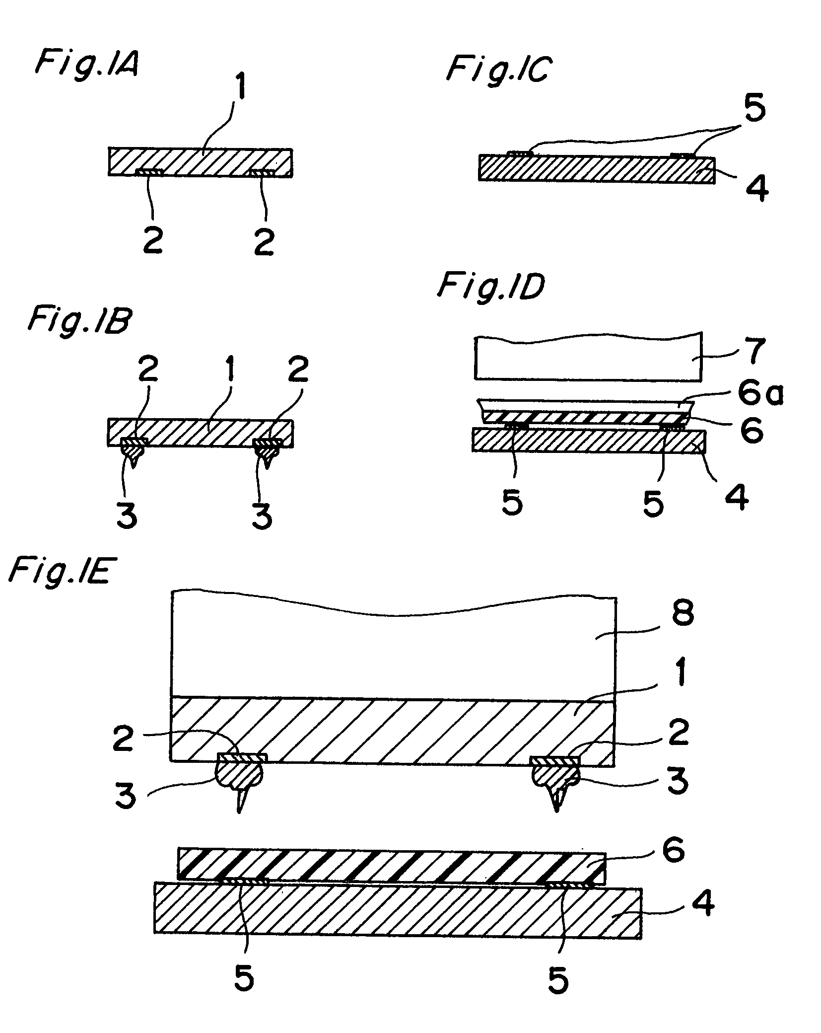
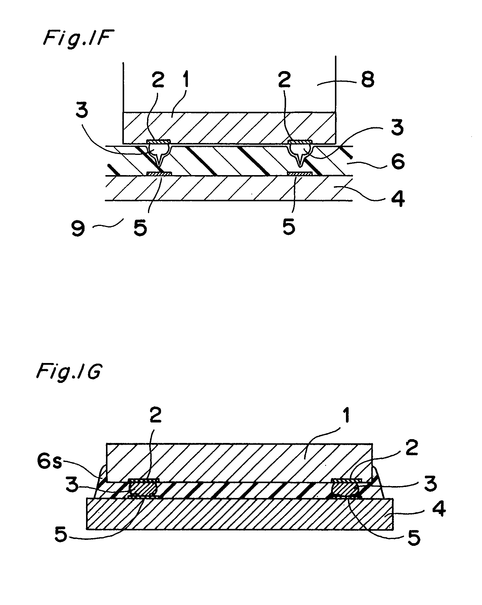
[0082]The method for mounting an IC chip on a circuit board according to the first embodiment of the present invention will be described with reference to FIG. 1A through FIG. 3C. On an IC chip 1 shown in FIG. 1A, bumps (protruding electrodes) 3 are formed on Al pad electrodes 2 of the IC chip 1 through the operations as shown in FIGS. 2A through 2F by a wire bonder. That is, a ball 96 is formed at the lower end of a wire 95 that is protruding from a holder 93 in FIG. 2A, and the holder 93 that is holding the wire 95 is moved down to bond the ball 96 to the electrode 2 of the IC chip 1, forming the approximate shape of the bump 3 as shown in FIG. 2B. In FIG. 2C, the holder 93 is started to move up with the wire 95 fed downward. The holder 93 is moved in an approximately rectangular loop 99 as shown in FIG. 2D to form a...

second embodiment

[0097]A mounting method and apparatus according to the present invention will be described with reference to FIGS. 7A through 7C and 8A through 8C. As described hereinabove, the protruding electrodes (bumps) 3 are formed on the electrodes 2 of the IC chip 1, while a sheet-shaped thermosetting resin or the thermosetting adhesive 6 having a shape dimension smaller than the outside dimension OL of the connection between the inner end edges of the electrodes 2 of the IC chip 1 is stuck to or coated on a center portion of the connection between the electrodes 5 of the circuit board 4, as shown in FIGS. 7B, 7C, and 8A. Next, the bumps 3 and the electrodes 5 of the circuit board 4 are aligned in position. As shown in FIG. 7A and FIG. 8B, the IC chip 1 is pressed against the circuit board 4 by the heated head 8 to harden the thermosetting resin or the thermosetting adhesive 6 interposed between the IC chip 1 and the circuit board 4 while simultaneously performing the warp correction of the ...

fourth embodiment

[0101]A mounting method and apparatus according to the present invention will be described with reference to FIGS. 10A through 10F. As shown in FIG. 10A, protruding electrodes (bumps) 3 are formed on the electrodes (pads) 2 on the IC chip 1 when mounting the IC chip 1 on the circuit board 4. On the other hand, as shown in FIG. 10B, a flux layer 12 is formed by coating and drying a flux component on one surface or both surfaces of the thermosetting resin sheet 6. Otherwise, the flux layer 12 is formed by sticking a flux component sheet formed by drying the flux component to the thermosetting resin sheet 6. The thermosetting resin sheet 6 having the flux layer 12 is stuck to the circuit board 4 as shown in FIG. 10C. In this case, the thermosetting resin sheet 6 is stuck so that the flux layer 12 comes in contact with the circuit board 4. Next, the bumps 3 are aligned in position with the electrodes 5 of the circuit board 4, and the IC chip 1 is pressed against the circuit board 4 by t...


PUM

PropertyMeasurementUnit
heightaaaaaaaaaa
pressureaaaaaaaaaa
temperatureaaaaaaaaaa

Abstract

When mounting an IC chip on a circuit board, bumps are formed on electrodes of the IC chip, and the bumps and the electrodes of the circuit board are aligned in position with each other with interposition of an insulative thermosetting resin having no conductive particle between the electrodes of the circuit board and the bumps. The IC chip is pressed against the circuit board with a pressure force of not smaller than 20 gf per bump by a heated head so as to perform warp correction of the IC chip and the board, while the resin interposed between the IC chip and the circuit board is hardened to bond the IC chip and the circuit board together.

Description

TECHNICAL FIELD[0001]The present invention relates to a method and apparatus for mounting an electronic component on a circuit board, i.e. for mounting an electronic component such as an IC chip and a surface acoustic wave (SAW) device singly (in the form of a bare IC in the case of the IC chip) on a printed circuit board to be used for an electronic circuit.BACKGROUND ART[0002]Nowadays, electronic circuit boards are employed in a variety of products, and they are improving in performance day by day. The frequencies to be used on the circuit boards are also increasing, and accordingly, the flip-chip mounting that ensures low impedance is the appropriate mounting method suitable for electronic devices that use high frequencies. In accordance with an increase in number of portable devices, the flip-chip mounting for mounting IC chips in the bare chip form, not in the package form, on a circuit board is needed. For this reason, the IC chips that are singly mounted on circuit boards and...

Claims


Application Information

Patent Timeline
Patent Type & Authority Patents(United States)
IPC IPC(8): H01L21/44H01L21/56H05K3/32H01L21/60H01L23/485H05K3/22
CPCH01L21/563H01L24/11H01L24/16H01L24/29H01L24/32H01L24/81H01L24/83H01L24/90H01L24/13H01L24/75H01L24/45H01L2224/0401H01L2224/05624H01L2224/1134H01L2224/13144H01L2224/1357H01L2224/1379H01L2224/138H01L2224/16225H01L2224/29078H01L2224/29399H01L2224/45144H01L2224/48624H01L2224/73203H01L2224/73204H01L2224/75H01L2224/75252H01L2224/81801H01L2224/83101H01L2224/83191H01L2224/83192H01L2224/83193H01L2224/838H01L2924/01004H01L2924/01009H01L2924/01013H01L2924/01014H01L2924/01029H01L2924/01033H01L2924/01046H01L2924/01047H01L2924/01052H01L2924/01078H01L2924/01079H01L2924/01082H01L2924/0781H01L2924/09701H01L2924/14H01L2924/3011H01L2924/3511H05K3/321H01L2224/2919H01L2924/00013H01L2924/01005H01L2924/01006H01L2924/01043H01L2924/014H01L2924/0665H01L2224/29101H01L2924/0132H01L2224/32225H01L2224/27436H01L2224/73104H01L2924/01028H01L2224/81395H01L2224/81191H01L2924/07811H01L2224/11334H01L2224/29076H01L2924/07802Y10T29/49144H01L2924/00014H01L2224/13099H01L2924/00H01L2924/15787H01L2924/181H01L2224/7598H01L2224/83851H01L2224/83855H01L2224/11822H01L2224/75251H01L2224/81048H05K3/32
Inventor NISHIDA, KAZUTO
Owner PANASONIC CORP
Learn More