Socket and contact of semiconductor package

a semiconductor and socket technology, applied in the field of sockets of semiconductor packages, can solve the problems of difficult elastic deformation of contacts, problems to be solved, and test or evaluation of semiconductor packages that cannot be performed with high precision in a high frequency range, so as to reduce the height of sockets, reduce self-inductance, and effectively utilize the full length

Inactive Publication Date: 2006-01-03
MOLEX INC
View PDF2 Cites 33 Cited by
  • Summary
  • Abstract
  • Description
  • Claims
  • Application Information

AI Technical Summary

Benefits of technology

[0014]An object of the present invention is to provide a socket of a semiconductor package, which may reduce self-inductance and enables high-density arrangement by reducing the height of the socket, and which also takes into consideration reduction of the cost and the contact reliability of a contact portion.

Problems solved by technology

This causes a problem that the test or evaluation of the semiconductor package could not be performed with high precision in a high frequency range.
Also, since most part of the one side of the contact piece 303 is pressingly contacted against the inner wall of a pressing inlet, it is difficult to elastically deform the contact.
However, there are problems to be solved as described below.
Namely, these are problems associated with the requirement of further reduction of height of the socket.
For this reason, there is a problem that it is difficult to further reduce the height thereof.
In the contact sheet described in the publication, since all the cantilevers are arranged on a planar surface with respect to the sheet, it is possible to ensure the advantage of the further reduction in height but there is a problem that the arrangement thereof at a high density is impossible.
As a result, the high density arrangement is impossible.
Also, conventionally, since the shape of the contact itself is complicated and a plurality of cantilevers are used for one spherical terminal, there is the problems that the assembling work takes long time and the cost is increased.

Method used


Image

  • Socket and contact of semiconductor package
  • Socket and contact of semiconductor package
  • Socket and contact of semiconductor package

Examples


Embodiment Construction

[0043]While the invention may be susceptible to embodiment in different forms, there is shown in the drawings, and herein will be described in detail, specific embodiments with the understanding that the present disclosure is to be considered an exemplification of the principles of the invention, and is not intended to limit the invention to that as illustrated and described herein.

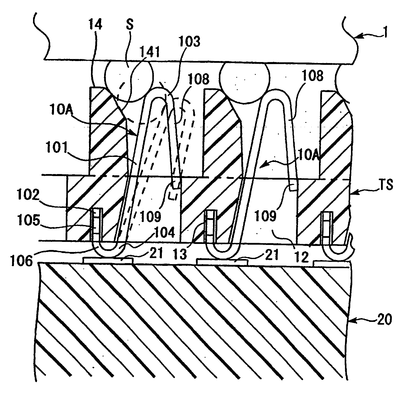
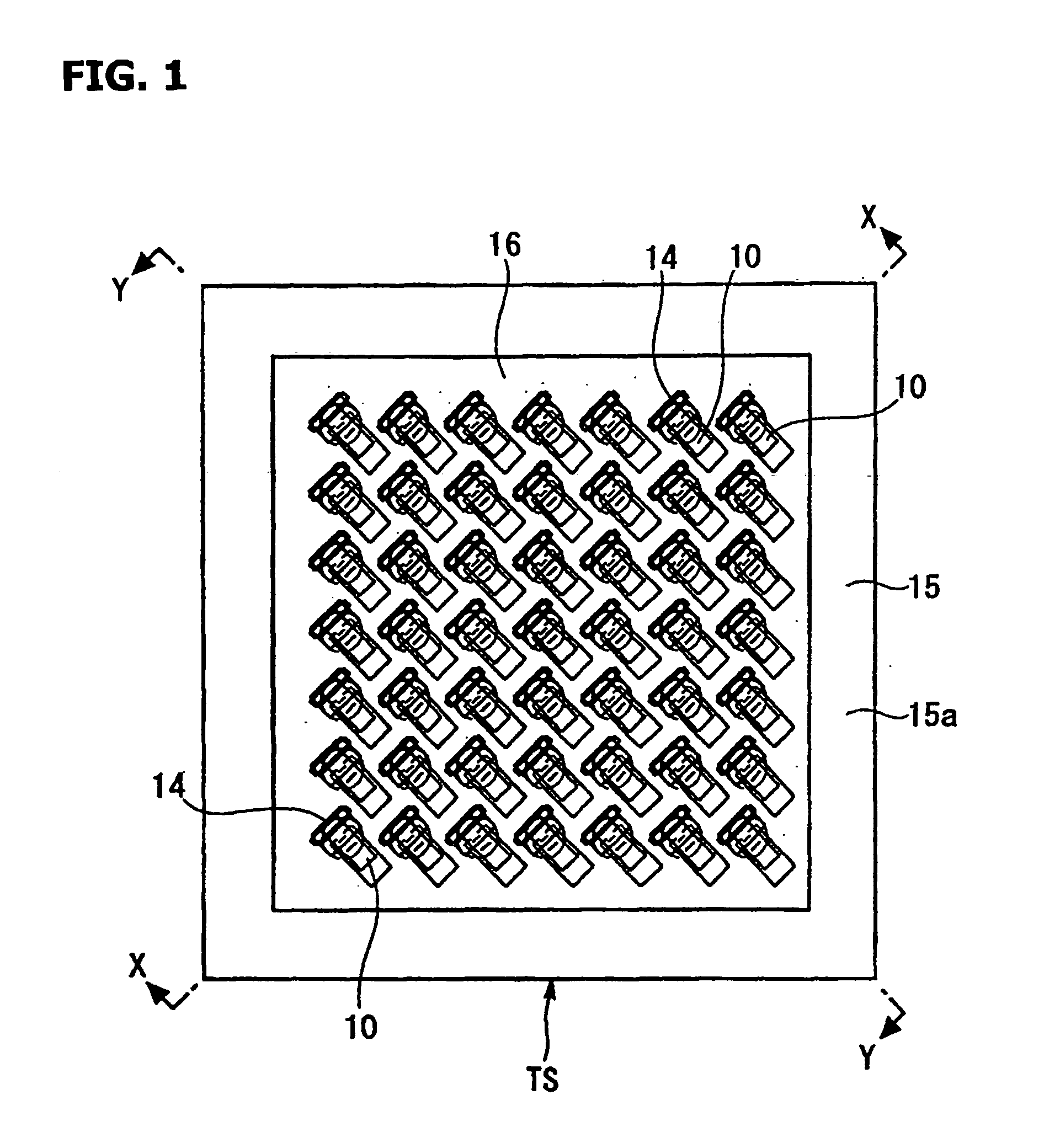
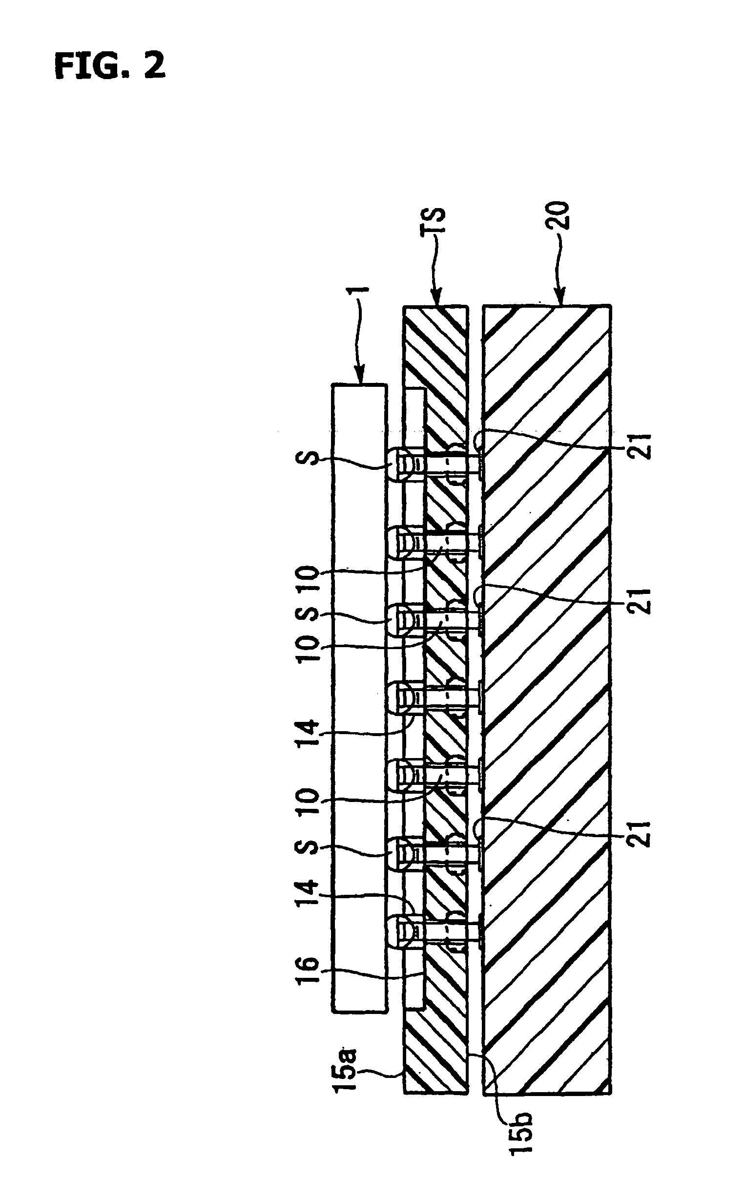
[0044]FIG. 1 is a plan view of a socket (test socket) of a semiconductor package in accordance with the embodiment of the present invention. FIG. 2 is a cross-sectional view taken along the line X—X of FIG. 1. FIG. 3 is a cross-sectional view taken along the line Y—Y of FIG. 1. FIG. 4 is an enlarged perspective view of a contact.

[0045]The test socket TS shown in these drawings is a BGA (Ball Grid Array) testing and evaluating socket of a semiconductor package 1 having a plurality of solder balls S arranged in an array on its one surface (bottom surface) side.

[0046]This test socket TS is provided with a pl...


PUM


Abstract

The present invention is directed to a socket connector (TS) having a plurality of contacts to be brought into contact with a plurality of solder balls (S) of a semiconductor package, a socket body (15) in which a mounting hole (11) is provided for each contact (10), a through-hole pierced in a height direction of the socket body and a contact support hole (13) are provided. Each contact (10) is provided with an upright piece (101) extending through the through-hole, a support piece extending from a proximal end side of the upright piece to be inserted into the through-hole and a contact portion (103) formed at a free end portion of the upright piece to be brought into contact with the solder ball. Each contact portion is arranged at a height level such that it projects from the surface of the socket body. A guide projection (14) is provided at a position to face an associated contact portion of each contact. These contact portion and guide projection are set at an interval such that the solder ball may be brought into contact with the both.

Description

FIELD OF THE INVENTION[0001]The present invention relates to a socket of a semiconductor package provided with a plurality of contacts to be brought into contact with a plurality of solder balls arranged on one side of the semiconductor package, and such contacts.BACKGROUND OF THE INVENTION[0002]Recently, the reduction of a pitch of integrated circuits has been advancing due to the demand of miniaturization of information processing equipment and high-speed performance thereof. In accordance with this, the actual mounting system is changing from a through-hole type to a surface mounting type and the arrangement of terminals is changing from a peripheral arrangement to an array arrangement. Furthermore, of such array arrangements, a ball grid array (BGA) in which solder balls are arranged in an array-like arrangement on a surface of a package is becoming a main type of a package on which the terminals may be mounted on the surface.[0003]In the case where a socket is used between a BG...

Claims


Application Information

Patent Timeline
Patent Type & Authority Patents(United States)
IPC IPC(8): H05K1/00G01R1/04
CPCG01R1/0483G01R1/0466
Inventor ADACHI, KIYOSHIYAGI, MASANORI
Owner MOLEX INC
Why Eureka
Try Eureka