Polymeric optical device having low polarization dependence and method of fabricating the same

a technology of polarization dependence and optical device, which is applied in the field of polymeric optical device, can solve the problems of limitation in an application, burden of developing a new material, and cannot be ignored, and achieve the effect of reducing polarization dependen

Inactive Publication Date: 2006-01-24
ELECTRONICS & TELECOMM RES INST
View PDF10 Cites 7 Cited by
  • Summary
  • Abstract
  • Description
  • Claims
  • Application Information

AI Technical Summary

Benefits of technology

[0008]The present invention is directed to a polymeric optical device capable of reducing polarization dependence by offsetting the stress effect, without using a specific polymer material.

Problems solved by technology

A polymeric optical device has a merit of easily being fabricated, but it has a limitation in an application thereof due to high polarization dependence as compared with the silica optical device, particularly, in the case of an arrayed waveguide grating (hereinafter, referred to as AWG) device.
Although the central wavelength difference of the silica AWG device is as low as about 0.35 nm, it cannot be ignored.
However, since most of the birefringence in the polymeric optical device is caused by the stress effect on the fabrication thereof, there is a burden of developing a new material.
Meanwhile, there is a difficulty in fabricating a polarization-insensitive AWG device, in the case of fabricating an optical device with a limited material.
But, in this case, since a specific polymer should be used as the substrate, it is difficult to fabricate it and to pack it with a different element.

Method used


Image

  • Polymeric optical device having low polarization dependence and method of fabricating the same
  • Polymeric optical device having low polarization dependence and method of fabricating the same
  • Polymeric optical device having low polarization dependence and method of fabricating the same

Examples


Embodiment Construction

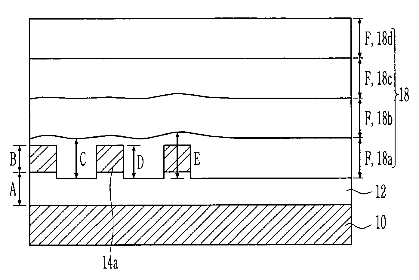
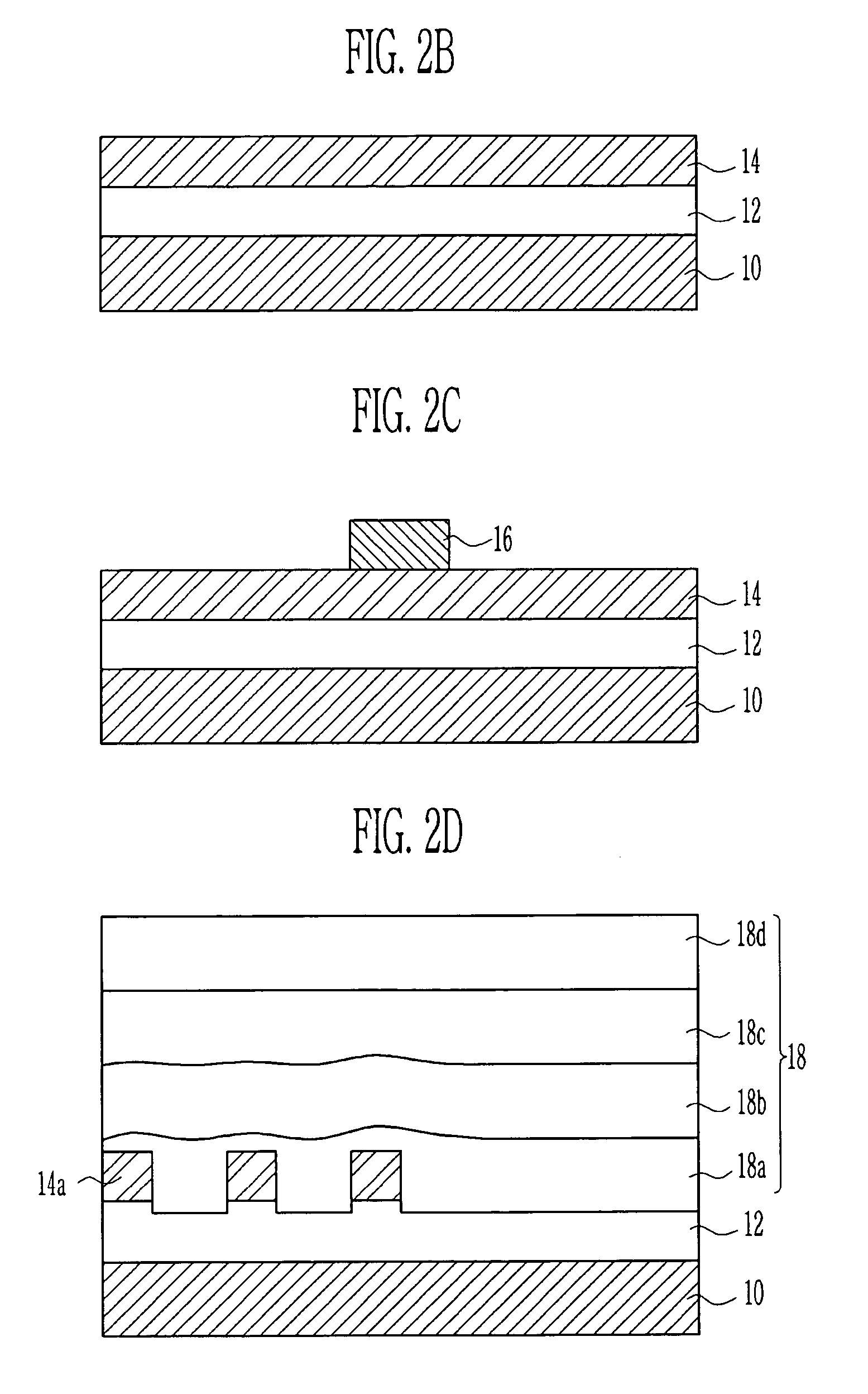
[0026]Hereinafter, the embodiments of the present invention will be explained with reference to the accompanying drawings. However, the embodiment of the present invention can be changed into a various type, and it should not be understood that the scope of the present invention is limited to the following embodiments. The embodiments of the present invention are provided in order to explain the present invention to those skilled in the art. Those having ordinary skill in the art and access to the teachings of the present invention will recognize additional modifications and applications within the scope thereof. It is therefore intended by the appended claims to cover any and all such applications, modifications, and embodiments within the scope of the present invention.

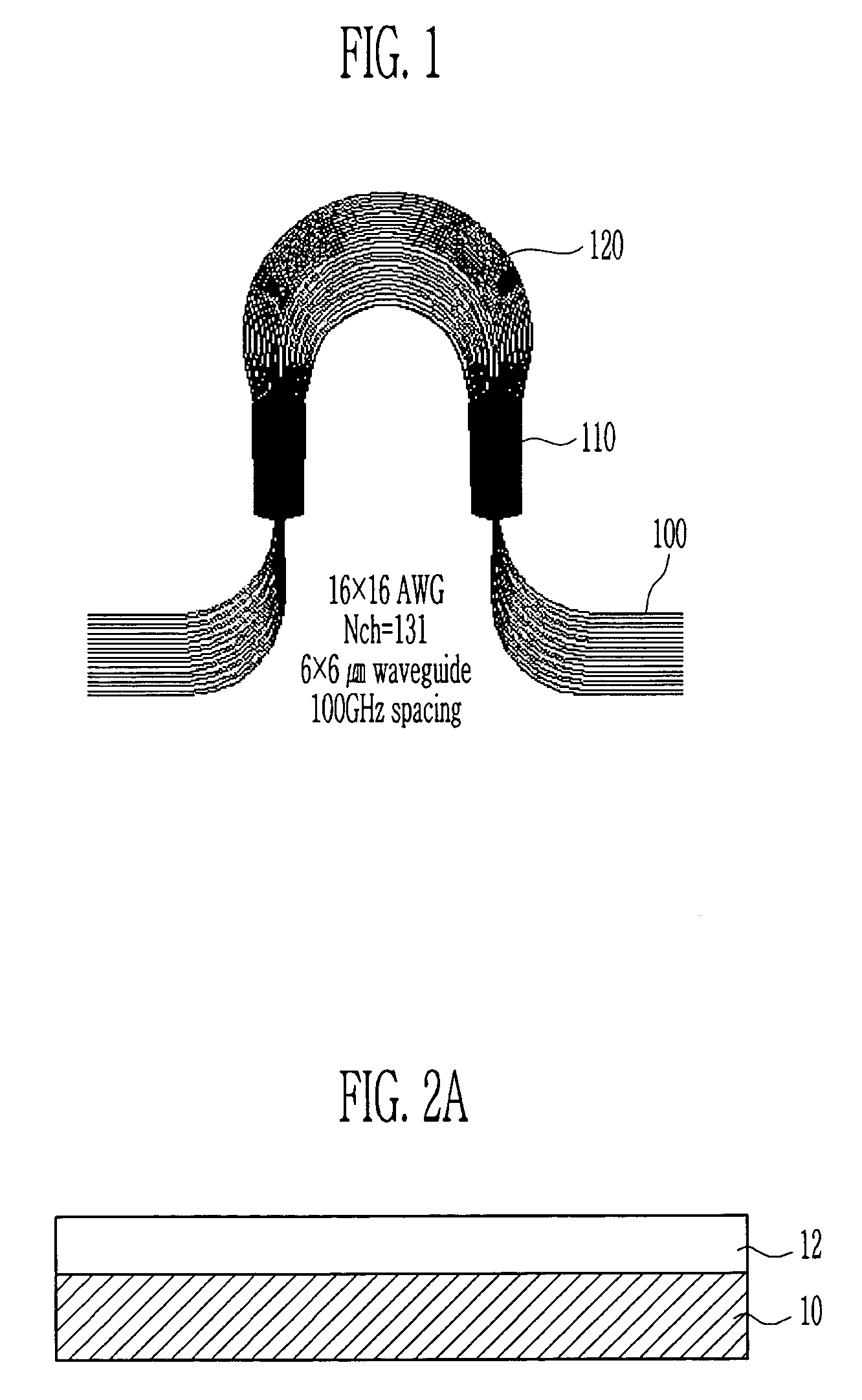
[0027]As shown in FIG. 1, an AWG according to a preferred embodiment of the present invention comprises an optical waveguide 100, a free propagation region 110, and a grating channel waveguide 120.

[0028]Hereinafter,...


PUM

PropertyMeasurementUnit
heightaaaaaaaaaa
central wavelengthaaaaaaaaaa
central wavelength shiftaaaaaaaaaa

Abstract

Provided is a polymeric optical device comprising a substrate, a lower cladding layer formed on the substrate, at least one core layer pattern formed on a predetermined region of the lower cladding layer and an upper cladding layer having at least two sub-upper cladding layers and formed on the lower cladding layer in which the core layer pattern is formed, and a method of fabricating the same, whereby birefringence of a polymeric optical device could be improved and polarization dependence could be reduced by adjusting the thickness of the sub-upper cladding layer and the number of stacks thereof.

Description

BACKGROUND[0001]1. Field of the Invention[0002]The present invention relates to a polymeric optical device and a method of fabricating the same, and more particularly, to a polymeric optical device and a method of fabricating the same capable of reducing variations of wavelength characteristics depending on polarization.[0003]2. Discussion of Related Art[0004]A polymeric optical device has a merit of easily being fabricated, but it has a limitation in an application thereof due to high polarization dependence as compared with the silica optical device, particularly, in the case of an arrayed waveguide grating (hereinafter, referred to as AWG) device. In case of an AWG fabricated by a silica material, a central wavelength difference according to a TE / TM polarization mode is about 0.35 nm (See H. Takahashi, Y. Hibino, and I. Niship, “polarization-insensitive arrayed-waveguide grating wavelength multiplexer on silicon”, Optics Lett., vol.17, no.7, pp499–501, 1992). In the case of an AW...

Claims


Application Information

Patent Timeline
Patent Type & Authority Patents(United States)
IPC IPC(8): G02B6/10G02B6/126G02B6/138G02B6/34
CPCG02B6/12023G02B6/138G02B6/126G02B6/1203
Inventor LEE, JONG MOOPARK, SUN TAKAHN, JOON TAEJU, JUNG JINLEE, MYUNG HYUNKIM, KYONG HON
Owner ELECTRONICS & TELECOMM RES INST
Why Eureka
Try Eureka