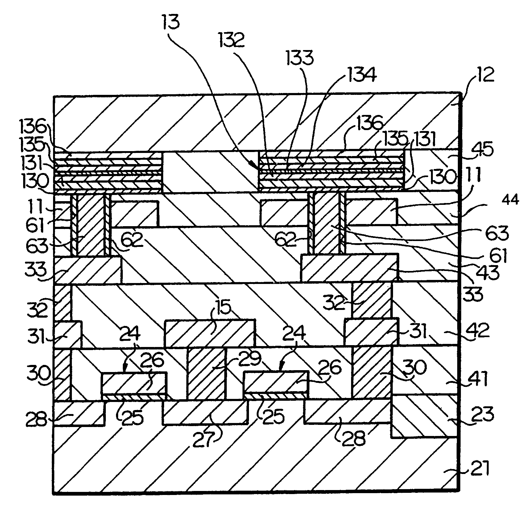
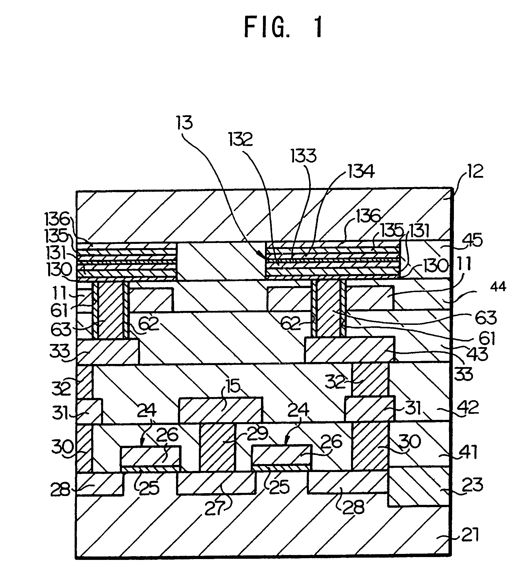
[0039]The above-mentioned second method for manufacturing the magnetic memory device further includes the step of forming the flux concentrator of the high permeability film so as to surround the opposite side faces of the first interconnection and an opposite face of the first interconnection to a side facing the tunnel magneto resistance element, so that a galvano-magnetic field generated at the time of applying a current to the first interconnection is concentrated efficiently on the storage layer (which will be also called a recording layer) of the tunnel magneto resistance element with the high permeability film formed on the opposite side faces of the first interconnection. Thus, it is possible to reduce current required for writing, thus reducing current consumption and also increasing lifetime of the first interconnection against electromigration. Further, there is less drive current required, which reduces an area of a current drive circuit, thereby providing an increased integration level. Furthermore, as leakage of magnetic field is also reduced, interference with adjacent cells is reduced.
[0042]The above-mentioned third method for manufacturing the magnetic memory device further includes the step of forming the flux concentrator of the high permeability film so as to surround the opposite side faces of the first interconnection and an opposite face of the first interconnection to the side facing the tunnel magneto resistance element, so that a galvano-magnetic field generated at the time of applying a current to the first interconnection is concentrated efficiently on the storage layer (which will be also called a recording layer) of the tunnel magneto resistance element with the high permeability film formed on the opposite side faces of the first interconnection. Thus, it is possible to reduce current required for writing, thus reducing current consumption and also increasing lifetime of the first interconnection against electromigration. Further, there is less drive current required, which reduces an area of a current drive circuit, thereby providing an increased integration level. Furthermore, as leakage of magnetic field is also reduced, interference with adjacent cells is reduced.
[0045]The above-mentioned fourth method for manufacturing the magnetic memory device may further include the step of forming the flux concentrator of the high permeability film so as to be located between the first interconnection and the tunnel magneto resistance element, while extending along the side face of the tunnel magneto resistance element through the insulator film, after a fabrication of the first interconnection, so that a galvano-magnetic field generated at the time of applying a current to the first interconnection is concentrated efficiently on the storage layer (which will be also called a recording layer) of the tunnel magneto resistance element with the flux concentrator formed on a lower side of the side face of the tunnel magneto resistance element. Thus, it is possible to reduce current required for writing, thus reducing current consumption and also increasing lifetime of the first interconnection against electromigration. Further, there is less drive current required, which reduces an area of a current drive circuit, thereby providing an increased integration level. Furthermore, as leakage of magnetic field is also reduced, interference with adjacent cells is reduced.
[0048]The above-mentioned fifth method for manufacturing the magnetic memory device further may further include the step of forming the first flux concentrator of the high permeability film so as to surround the opposite side faces of the first interconnection and an opposite face of the first interconnection to the side facing the tunnel magneto resistance element, and the step of forming the second flux concentrator of the high permeability film so as to be located between the first interconnection and the tunnel magneto resistance element while extending along the side face of the tunnel magneto resistance element through the insulator film, after a fabrication of the first interconnection, so that a galvano-magnetic field generated at the time of applying a current to the first interconnection may be concentrated efficiently on the storage layer (which will be also called a recording layer) of the tunnel magneto resistance element through a transfer from the first flux concentrator to the second flux concentrator. Thus, it is possible to reduce current required for writing, thus reducing current consumption and also increasing lifetime of the first interconnection against electromigration. Further, there is less drive current required, which reduces an area of a current drive circuit, thereby providing an increased integration level. Furthermore, as leakage of magnetic field is also reduced, interference with adjacent cells is reduced.
[0050]The magnetic memory device manufactured by the method according to the preferred embodiments of the present invention may eliminate a need to fabricate a conventionally required extraction interconnection part connected to the tunnel magneto resistance element, thereby enabling a decrease of a length in parallel to an array of the second interconnections (bit lines) without newly creating an area of the contact allotted to the cell area. Specifically, when a minimum line width is assumed to be F, the conventional magnetic memory device has required a cell area having a size equal to or more than 8F2, whereas the magnetic memory device of the present invention is obtainable in a cell size smaller than 8F2. More specifically, the cell size of the magnetic memory device of the present invention is minimized to 4F2, for instance. Thus, there may be provided a MRAM composed of one switching element and one TMR element, in which the same access rate as the conventional MRAM or magnetic memory device of one witching element-one TMR element type is maintained, and a more reduction in cell area as compared with the conventional magnetic memory device is enabled. A cell area of the MRAM composed of one switching element and one TMR element is made smaller as much as a cell area of the cross-point MRAM. The magnetic memory device having the flux concentrator may also produce the above effects likewise.
[0051]Further, because of no need to fabricate the conventionally required extraction interconnection part connected to the tunnel magneto resistance element, single etching is applicable to form the tunnel magneto resistance element. Thus, there is no need to take a margin of a mask alignment into consideration in fabricating the extraction interconnection, thereby enabling a further proportional reduction in cell area. Further, an applicability of single etching to form the tunnel magneto resistance element requires no fine control of etching such as suspension of etching on the tunnel barrier layer, the fixed magnetization layer or the anti-ferromagnetic layer, thereby enabling a decrease of a load on an etching process.


